I would like to place an order for the 3’’ Semi-insulating Silicon Carbide (SiC) thickness of 350um ,Double side polished, 4H/25 pieces. Btw, do you have data sheet for that to share? Would like to know more about the electrical/thermal properties and surface finishes about the wafer. Thanks.
Silicon Carbide Wafers & SiC Epitaxy
Silicon Carbide Wafers for University Research
A PhD candidate recently requested a quote for the following:
Please reference #259893 for pricing.
Get Your SiC Wafer Quote FAST!
Difference Between Prime and Research Grade Silicon Carbide Wafers
The difference of Prime grade and Research grade SiC:
- “Prime grade” with useable area>/=90%,defect density i.s MPD</=5/cm^2,resistivity uniformity >/=90%, best "thickness, warp & bow" value, No Surface defects
- “Research grade” with useable area>/=80%,defect density i.s MPD</=10/cm^2, resistivity uniformity >/=80%, better "thickness, warp & bow" value, Very few and small Surface defects
4H Silicon Carbide (SiC) Wafer Applications include
4H-N SiC Substrates/SiC Epitaxy
• Optoelectronics
• Power-factor correction
• Solar inverters
• Industrial motor drives
4H-HPSI SiC Substrates/III-Nitride Epitaxy
• High-power RF
• Graphene
• Terahertz
What is Poly Silicon Carbide?
Polycrystalline silicon carbide, also known as poly-SiC, is a compound of silicon and carbon. Silicon carbide (SiC) has been used in various applications due to its excellent properties, such as its hardness, high temperature resistance, chemical resistance, and high thermal conductivity.
In a polycrystalline state, a material consists of numerous small crystalline regions or grains, each of which may have a different orientation, which can affect its overall properties. The manufacturing process can greatly influence the properties of polycrystalline materials.
Poly-SiC is used in a variety of applications, including electronics, due to its semi-conducting properties, and in mechanical systems where high-temperature stability, hardness, and chemical resistance are necessary. It's particularly prevalent in power electronics, such as power semiconductors, due to its high breakdown electric field strength and high thermal conductivity, which can enhance system performance and reliability.
As of my knowledge cutoff in 2021, research continues to explore new uses for Poly-SiC and ways to improve its manufacturing processes.
100mm 4H SiC Sale!
We have a large selection of inexpensive test grade silicon carbide wafers for research and production.
Buy Online SiC Item #3912 - 100mm N+ Nitrogen Doped SiC Wafer 4 deg off-axis 350 micron
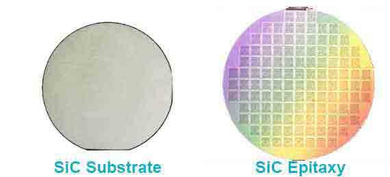
Silicon Carbide (SiC) Substrate and Epitaxy
Buy Online and SAVE! See bottom of page for some of our SiC inventory.
SiC substate (epi ready), N type and Semi-insulating,polytype 4H and 6H in different quality grades, Micropipe Density (MPD):Free, <5/cm2, <10/cm2, <30/cm2,<100/cm2
SiC Epitaxy:Wafer to wafer thickness uniformity: 2% ,Wafer to wafer doping uniformity: 4%.

Current Inventory Includes, but not limited to the following. We also have < 25.4mm, 25.4mm, 76.mm, 100mm available.
<6H-N
<50.8mm N/Nitrogen <0001>+/0.5 deg 330um 0.02 ~ 0.2 Ω·cmSSP Epi Ready Roughness <0.5nm
<4H-N
<50.8mm N/Nitrogen <0001>+/-0.5 deg 330um 0.01-0.1 Ω·cm SSP Epi Ready< Roughness : <0.5 nm
Please provide us with your specs or ask to see our inventory! Below are just some of the SiC wafers that we have in stock.
Buy as few as one Silicon Carbide Wafer (SiC) Wafer!
2" Silicon Carbide (SiC) 6H N-Type Epi-Ready
2" dia, 6H-N
Type/ Dopant : N / Nitrogen
Orientation : <0001>+/-0.5 degree
Thickness : 330 ± 25 um
D Grade,MPDä100 cm-2 D Grade,RT:0.02-0.2 Ω·cm
Single face polished/Si face epi-ready with Chemical Mechanical Polish (CMP),Surface Roughness : <0.5 nm
2" 6H N-Type
6H-N 2" dia, Type/ Dopant : N / Nitrogen
Orientation : <0001>+/-0.5 degree
Thickness : 330 ± 25 um
B Grade,MPDä30 cm-2 B Grade,RT 0.02 ~ 0.2 Ω·cm
Single face polished/Si face epi-ready with CMP,Surface Roughness : <0.5 nm
2" Silicon Carbide (SiC) 4H N-Type Epi-Ready
2" 4H N-Type
4H-N 2" dia, Type/ Dopant : N / Nitrogen
Orientation : <0001>+/-0.5 degree
Thickness : 330 ± 25 um
D Grade,MPDä100 cm-2 D Grade:RT:0.01-0.1 Ω·cm D Grade,Bow/Warp/TTV<25um
Single face polished/Si face epi-ready with CMP,Surface Roughness : <0.5 nm
2" Silicon Carbide (SiC) 4H N-Type N-type Nitrogen Doped
4H-N 2" dia, Type/ Dopant : N / Nitrogen
Orientation : <0001>+/-0.5 degree
Thickness : 330 ± 25 um
B Grade,MPDä30 cm-2 B Grade:RT:0.01 - 0.1 Ω·cm B Grade,Bow/Warp/TTV<25um
Single face polished/Si face epi-ready with CMP,Surface Roughness : <0.5 nm
3" Silicon Carbide (SiC) 4H N-Type
4H-N 3" dia, Type/ Dopant : N / Nitrogen
Orientation :4 degree+/-0.5 degree
Thickness : 350 ± 25 um
D Grade,MPDä100 cm-2 D Grade,RT:0.01-0.1Ω·cm D Grade,Bow/Warp/TTV<35um
Double face polished/Si face epi-ready with CMP,Surface Roughness : <0.5 nm
3" 4H N-Type
4H-N 3" dia, Type/ Dopant : N / Nitrogen
Orientation : 4 degree+/-0.5 degree
Thickness : 350 ± 25 um
B Grade,MPDä30 cm-2 B Grade,RT:0.01 - 0.1Ω·cm B Grade,Bow/Warp/TTV<35um
Double face polished/Si face epi-ready with CMP,Surface Roughness : <0.5 nm
3" 4H SI
4H-SI 3" dia, Type/ Dopant : Semi-insulating / V
Orientation : <0001>+/-0.5 degree
Thickness : 350 ± 25 um
D Grade,MPDä100 cm-2 D Grade,RT:70 % ≥1E5 Ω·cm
Double face polished/Si face epi-ready with CMP,Surface Roughness : <0.5 nm
3" 4H SI
4H-SI 3" dia, Type/ Dopant : Semi-insulating / V
Orientation : <0001>+/-0.5 degree
Thickness : 350 ± 25 um
B Grade,MPDä30 cm-2 B Grade,RT:80 % ≥1E5 Ω·cm
Double face polished/Si face epi-ready with CMP,Surface Roughness : <0.5 nm
2" Semi Insulation Silicon Carbide 6H
2" 6H SI
6H-SI 2" dia, Type/ Dopant : Semi-insulating / V
Orientation : <0001>+/-0.5 degree
Thickness : 330 ± 25 um
D Grade,MPDä100 cm-2 D Grade,RT:70 % ≥1E5 Ω·cm
Single face polished/Si face epi-ready with CMP,Surface Roughness : <0.5 nm
2" 6H SI
6H-SI 2" dia, Type/ Dopant : Semi-insulating / V
Orientation : <0001>+/-0.5 degree
Thickness : 330 ± 25 um
B Grade,MPDä30 cm-2 B Grade,RT:85 % ≥1E5 Ω·cm
Single face polished/Si face epi-ready with CMP,Surface Roughness : <0.5 nm
4" N-type Silicon Carbide (SiC) 4H
4" 4H N-Type
4H-N 4"dia.(100mm±0.38mm),
Type/ Dopant : N / Nitrogen
Orientation : 4.0°±0.5°
Thickness : 350μm±25μm
D Grade,MPDä100 cm-2 D Grade,0.01~0.1Ω•cm D Grade,TTV/Bow /Warp<45um
