Silicon-on-Insulator (SOI) Wafers for Research & Production

university wafer substrates

What SOI Wafer Spec Do I Need?

There are many different types of silicon on insulator wafers, so how do you know which one to choose?

A scientist requested a quote for the following:

I'm planning on using an SOI wafer in which I will be making 100um wide by 400um deep (till the BOx) vias, which I would then be passivating with either PECVD or Sputtered a-SiC or Oxide. It was suggested that you could help me with the supply of SOI wafers, and also with your sputter deposition services. It would be great if you could send me a quote for a box of SOI wafers with undoped Si handle and device layers, the handle being 400um thick and the device layer being as thin as you can make it. I would like the BOx to be 2-5um thick. And for the sputtering, Im looking at depositing 500A thick layer to passivate my vias. It would be nice if you could supply me information on your oxide and carbide films.

Reference RFQ#253215 for specs/pricing.

Start Researching Today! Buy Online!

It can be hard to decide which silicon on insulator soi wafer is right for your needs. Each type of bonded or simox wafer has its own advantages and disadvantages.

Our silicon on insulator wafers are the best option for most applications. We offer a variety of bonded and simox wafers, so you can find the perfect fit for your needs. Our products are backed by our commitment to quality and customer service. Buy as few as one wafer or even a diced piece!

Get your SOI Quote FAST! Or, Buy Online and Start Researching Today!

Company:

SOI Wafers to Fabricate 2D Devices

SOI wafers are composed of the wafer handles, providing mechanical strength in the manufacturing process, a device layer on/inside the device being manufactured, and a Buried Oxide layer (BOX) that separates the device layer from the handle wafers (see A). An SOI MOSFET is a metal-oxide-semiconductor field-effect transistor (MOSFET) device where the semiconductor layer, which can be either silicon or germanium, is formed over the insulator layer, which can be the buried oxide layer (BOX) formed on a semiconductor substrate. 

Scientists have used the following SOI wafer for their experiments.

Item # 2551:
200mm SOI Type: P Dopant: B
Orientation: <100>
Resistivity: 1-20O/cm
Thickness: 725+/-25um
Device / Oxide thickness nm
70 / 2000

Buy online or send us the specs you would like us to quote.

Silicon on Insulator (SOI) Wafers

Using silicon on insulator (SOI) wafers in microprocessors is becoming more popular. These types of semiconductors are more efficient and can improve the speed and power of microprocessors. SOI wafers are relatively expensive, but they can make up for this cost in process savings. The cheapest SOI wafers are usually around 100mm in diameter, other diameters are also availalble.

We specialize in Small quantities orders!Diced Silicon on Insulator Wafers

We also sell diced pieces of expensive Soitec and Simox wafers. You need to increase your semiconductor device’s performance by decreasing electrical losses. SOI wafers is the solution. SOI reduces the power required and heat that’s generated, thus increasing the device’s efficiency and speed.  SOI insulation, or oxide layer, thickness depends on the application.  Thermal oxide from a few nanometers thick to many microns can be used in microelectronics as it reduces short-channel effects. Silicon on insulator wafers  operate at lower temperature to doping. Higher device yield can be had because of SOI’s higher density.

SOI applications include

  • Silicon Photonics
  • Microelectronic Devices
  • Radio Frequency (RF) Devices

Silicon-on-Insulator for fabricating Silicon Waveguides

Researchers have been using the following specs to fabricate the following SOI wafers as there is no additional absorbtion loss due to doping in integrated photonics work.

  • Silicon Waveguides
  • Grating Couplers
  • Integrated Photonic Components

SOI Item #3536
25mm X 25mm P/B <100> 10-20 ohm-cm 725um SSP Prime

Other wafer diameters and dimensions are also available

UniversityWafer, Inc's silicon-on-insulator (SOI) wafers , can be used the following electronics applications:

  • ultra-low power signal processing
  • wireless connectivity
  • power, image sensors and silicon photonics applications
  • radio-frequency silicon-on-insulator (RF-SOI) substrates
  • ultra-low power connectivity RF

UniversityWafer, Inc. can provide researchers with a wide range of engineered substrates including fast growing segments like automotive, AI-IoT (AIoT) and 5G.

Bonded Silicon-on-Insulator for Nanomaterials Research

Researchers have used the following SOI wafer item to research nanomaterials (applied physics) for quantum/photonic computation.

Si Item #3213
150mm P/B <100> 675um SSP
Device Layer: 2um Device Res 17-23 ohm-cm
Oxide: 0.5um
Handle Layer: 675um Res 4.8-7.2 ohm-cm

SOI Wafer for Silicon Waveguides

Research clients have used our Silicon-on-Insulator wafers for their silicon waveguide research.

SOI Item #3536
25mm X 25mm P/B <100> 10-20 ohm-cm 725um SSP Prime
SOI square, Device: 220nm, BOX: 3000nm Handle thick: 725+/-15um, TTV: <1um

What Are Silicon on Insulator Applications?

Silicon on insulator (SOI) is used for many applications in electronics. These include mixed-signal applications, microprocessors, and RF waveguides. Here's a brief overview of what SOI is and how it's used. It's a promising material with many applications and is becoming more prevalent.

RF and mixed-signal applications

The global RF and mixed-signal applications of silicon on insulator market is segmented by application, region, and technology. The North American region accounts for the largest share of the industry. The growing automotive industry is a major driver. The Middle East and Africa region is expected to grow at the highest CAGR during the forecast period.

RF and mixed-signal applications of semiconductors are found in cellular technology, consumer electronics, and industrial applications. RF and mixed-signal applications require advanced manufacturing technologies to integrate passive elements with digital functionality. Embedded non-volatile memories, optical elements, and bipolar elements can be used in these mixed-signal devices.

The semiconductor on insulator technology reduces junction capacitance and power consumption, resulting in higher performance and lower power. The resulting silicon-on-insulator chips can operate up to 15 percent faster than bulk CMOS chips. The technology also increases the device's speed and power.

Silicon-on-insulator devices can be manufactured using several methods. One technique uses seed methods, which grow the topmost layer of silicon directly on the insulator. A silicon-on-insulator device is produced using a diamond-tipped tool.

The high-purity and uniformity of the semiconductor are necessary for RF devices. The thickness of the substrate is also crucial for the frequency response. Hence, the substrate and the RF components must be optimized together. However, the RF devices and the substrate specifications can vary significantly over time, so it is crucial to account for this variability when designing the device. One way to minimize the variability is to use engineered substrates.

RF waveguides

The global silicon on insulator market is segmented into three segments: technology, application, and region. In terms of region, the North American region is the largest region, accounting for approximately 80% of the total market. Europe, meanwhile, is split into three sub-regions: Italy, France, and the rest of Europe. Moreover, the Asia-Pacific region is further segmented into South Asia and Latin America. The Middle East and Africa region is likewise segmented into two segments: type and size.

The process of silicon on insulator fabrication is relatively simple and is cost-effective, requiring minimal labor and materials. It also allows for the precise control of the silicon layer thickness, which improves device performance and protection from environmental factors. These are just a few of the advantages that silicon on insulator fabrication offers.

Silicon on insulator waveguides are a promising technology for RF and optical applications. The technology has several benefits over traditional silicon waveguides, including the ability to integrate multiple functionalities on a single chip. For example, silicon waveguides can be used to build ultra-high-frequency antennas.

The silicon on insulator market is segmented by technology, application, product, and region. Automotive and consumer electronics are among the leading applications for silicon on insulators. The automotive and consumer electronics segments are experiencing rapid growth. The technology used to make silicon on insulators is very versatile and can be customized to meet specific needs of different industries.

RF amplifiers

The silicon on insulator market is segmented based on technology, region, and application. In 2018, the North American market held the largest share, followed by the European market (including the United Kingdom, France, and Italy), and the Asia-Pacific market (including Latin America and the GCC). In addition, the Middle East and Africa market is expected to witness significant growth over the next five years.

The number of transistors used in silicon on insulator (SOI) power amplifiers is limited by the breakdown voltage, which typically ranges from 80 to 300V. The breakdown voltage reduces the signal current of each transistor, which results in an improved amplifier efficiency. However, this approach is only effective when the two silicon layers have identical phase.

Another advantage of SOI technology is the ability to integrate the components within a single chip. The SOI layer eliminates the need for a metal interconnect. This helps reduce the cycle time for manufacturing products. SOI technology is also capable of reducing RF losses significantly.

Another benefit of SOI technology is the ability to make high-frequency devices. RF amplifiers using SOI devices need wideband power, and SOI technology is ideally suited for this purpose. In order to achieve this, dynamically-biased silicon transistors are used in stacks with different topologies. This reduces gate oxide breakdown and improves output power. Moreover, the power performance of SOI devices is enhanced by the incorporation of series-connected transformers.

RF transceivers

SOI is an excellent choice for RF transceivers due to its superior performance characteristics. It offers superior insertion loss and linearity while providing CMOS efficiency and a low power envelope. In addition, it enables faster data transmission for applications such as vehicle-to-vehicle communications and virtual reality. Furthermore, it is cost-effective and allows for the stacking of multiple power amplifiers in a single chip.

The process for silicon on insulator devices is based on a two-layer process. The first layer is oxidized, while the second layer is deposited on top. This step-by-step process is referred to as Smart Cut, and involves controlled exfoliation and ion implantation.

The second layer consists of a transistor and a capacitor. These are connected serially. This enables the device to have an integrated transmitter and receiver. Additionally, it has body-bias capability, which allows it to provide superior performance and energy efficiency. It also offers superior reliability in automotive applications.

SOI provides high resistivity properties, which helps reduce substrate losses. It can reach values as high as 1 kO*cm. This makes SOI a promising substrate for RF integrated circuits and mixed-signal applications. In addition, its low-power consumption and wide-band capability make it a valuable choice for mobile electronics and other RF transceivers.

CMOS technology is another option for RF transceivers. It allows for multiple active devices and has a high-Q factor. In addition, the process also enables high-value poly resistors, high-current inductors, and MOM capacitors.

Radio Frequency (RF) Filters

RF filters using silicon on insulator (SOI) technologies have several advantages over conventional RF filters. This technology allows for small footprints, high power handling, and an extensive tuning range. It also has the advantage of avoiding the nonlinearities of varactor filters and the size limitations of switched filter banks. This type of RF filter can also be programmed via a three-wire serial control interface. Its features include a five-bit tuning resolution, center frequency and bandwidth tuning, and reflection coefficient tuning. In addition to these advantages, the power consumption of this type of RF filter is less than 50 mW.

RF filters using SOI substrates can also be mounted as flip-chip components. The flip-chip mounting method helps minimize signal loss that occurs between the SOI substrate and the filter. This type of mounting also allows for higher performance and reduced parasitics. In addition, SOI substrates are inexpensive and are suitable for use in devices with high sensitivity.

A thin layer of silicon is used as the core of the filter. The SOI layer has a high refractive index and a small footprint. It is also capable of multifunctionality on a single chip. However, silicon waveguides are sensitive to fabrication defects and sidewall roughness, which can increase the loss and induce phase error.

Video: Silicon on Insulator Tech


Silicon-on-Insulator Applications

SOI applications include:

  • RF Filters
  • Optoelectronics
  • Image Sensing
  • Wireless Connectivity
  • Flexible-Hybrid Electronics
  • RF MEMS

End Markets Include:

What are Common SOI Wafer Specs Used to Fabricate Microfluidic Devices

A process integration engineer need to find the right soi wafer specs for microfludic device fabrication. He requested we quote the following:

I'm looking for 1-2 SOI wafers or pieces on the order of 2+ cm in size. Si device layer ~500 nm and oxide thickness >5 um (all glass substrate ok). Does not have to be prime grade. The project will probably be in two stages:
  1. check autofluorescence of the material in an inverted microscope so small pieces or 2" wafers, relatively thin box, ok
  2. whole wafers for processing with thick box so we can remove all the Si substrate (backgrind??) and end up with ~100um thickness chips with device layer (~500 nm Si) on oxide (the box of the SOI wafer).
Other than that the device layer can be P or N type, highly doped 0.01 Ohm-cm, at least test grade. The wafers will be used for microfluidics type project, not making semiconductor devices. It is better for us actually to have 500 nm Si on a glass wafer but I figure those wafers will be harder to find.

Reference #251891 for specs and pricing.

Why Use SOI Wafers to Fabricate Microfluidic Devices?

Silicon on insulator (SOI) wafers have become the most commonly used substrate for microfluidic dev. This is because they provide a number of advantages for the fabrication of these chips. The main advantage is that they improve the speed and efficiency of the chip. The other advantage is that they have a high device yield.

The SOI insulating oxide is then bonded to the upper silicon layer via bonding technology. This process typically uses ion implantation to create the insulating oxide layer directly under the silicon surface and exfoliation to control the thickness of the silicon layer.

These processes allow the silicon layer to be precisely etched, which ensures that it is uniformly etched. The etching rate varies from 0.8 mm/min to 1.25 mm/min depending on the width and aspect ratio of the cavities.

For microfluidic dev, this type of SOI insulating oxide is often used in conjunction with Dry Reflow Etching (DRIE). DRIE etching removes very precise amounts of silicon to create the desired cavities defined by a photomask.

This method is very easy and allows for the precise control of the silicon layer thickness, which improves device performance and reduces environmental exposure. The resulting device is also less power-hungry than similar devices fabricated on traditional silicon substrates. This is especially important for low-power applications. SOI insulators are also known for their ability to form a low-loss waveguide in RF and optical applications.

SOI Rib Waveguide

A masters student requested the follwoing quote:

I have checked them, and I think that SOI with ID 1811 is suitable for us, but the SOI thickness is only 220 nm. We just wondering that too thin for our research, because we will use SOI rib waveguide with the total thickness is around 400 nm or 500 nm (the detail design as attached file).

For the future project, we also want to add the grating (pitch grating around 254 nm) in the SOI rib waveguide.
So, is it possible if we will order with the grating layer in the SOI waveguide?

The second question is could the university wafer also build the SOI active layer? or is it special only for SOI passive layer?

A Silicon-on-Insulator (SOI) rib waveguide is a type of optical waveguide that is widely used in silicon photonics due to its ability to tightly confine light. It's based on the SOI technology, a type of fabrication method used in semiconductor industry where a thin layer of silicon (the top layer) is placed on an insulator, typically Silicon Dioxide (SiO2).

The term "rib" refers to the specific structure of the waveguide. The rib waveguide is a ridge or a "rib" of silicon that sits on top of the silicon layer, surrounded by the insulator, creating a three-layer structure: silicon (rib) - silicon - insulator.

The light is guided down the silicon rib, and because of the refractive index difference between the silicon and the insulator, the light is effectively confined within the silicon rib. This allows for efficient transmission of the light with low losses.

SOI rib waveguides are often used in various integrated optical circuits, including modulators, detectors, multiplexers, etc. due to their high performance and compatibility with existing silicon-based manufacturing techniques.

Reference #237913 for specs and pricing.

What is SOI Passive Layer?

in a Silicon-on-Insulator (SOI) technology, the "passive" layer typically refers to the insulator layer, which is often composed of silicon dioxide (SiO2) or some other material with a low refractive index. This layer is called "passive" because it does not actively participate in guiding the light (as the silicon "rib" does in a waveguide) or in electronic conduction, but it plays a critical role in the overall device structure and performance.

The SOI structure is usually a three-layered stack: a thin silicon layer (the device layer where the active devices like transistors or waveguides are built), the insulating layer (also known as the buried oxide or BOX layer), and a thicker silicon layer (the substrate or handle layer).

The role of the passive (insulating) layer in the SOI technology is to electrically isolate the top thin silicon layer (where the active devices are located) from the bottom silicon substrate. This isolation can improve the performance of the active devices, reduce power consumption, and mitigate various parasitic effects often encountered in traditional silicon technologies. In terms of optical waveguides, the insulator layer also helps confining the light within the guiding layer (top silicon layer), providing efficient light transmission.


SAVE on Expensive Soitec SOI SOITEC SOI Wafers and Simox SOI wafers DICED into small and affordable pieces!

Bonded SOI Wafers made to order in small quantiles and short lead times.soi wafers in a cassette
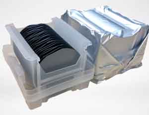
We work with several SOI manufacturers to provide small quantities of SOI to you. Whole wafers and diced pieces available at a deep discount

For example we have a potential order for 50 of the following:

100mm P/B (100) 500um 10-20 ohm-cm Prime Grade
Device 340nm
Oxide 1,000nm

The manufacturer's minimum quantity is 50 wafers. But you only need say 1-3 wafers. We could potential buy 50 and sell you just a few at a very reasonable cost.

Other diameters such as 150mm is also possible. If this interests you, please let us know. Or fill out the form below and let us know which specs you need!

Below are just some of our Thin Device Layer SOI Inventory

ID Diam Type Dopant Orien Res (Ohm-cm) Thick (um) Polish Grade

Device: 220 nanometers, BOX: 3000nm Handle thick: 725+/-15um, TTV: <1um

3536 25mm X 25mm P B <100> 10--20 725um SSP Prime

Device 2.2um BOX, 27.5 micron Device. Handle Res: 1000-2000 ohm-cm, Device Res: 0.004-0.006 ohm-cm

3308 100mm P B <100> 1000-2000 483um SSP Prime

Device Layer: 2um, Oxide: 0.5um, Handle Layer: 675um. Device Res 17-23 ohm-cm, Handle Res 4.8-7.2 ohm-cm

3213 150mm P B <100> 10--20 675um SSP Test

Device Layer: 220nm, Oxide: 2um, MFR PN: SMB-6P675-2-0.22

3381 150mm P B <100> 10--20 675um SSP Prime

Device thickness: 70nm, Oxide thick: 2000nm

2551 200mm P B <100> ~1-20 725um SSP Prime

Device: 220nm, BOX: 3,000nm

3523 200mm P B <100> 10--20 725um SSP Prime

SIMOX Silicon-on-Insulator SOI

We have the following thin device layer SOI available in small and large quantities. Please fill out the form for an immediate quote.

100mm SOI WAFERS

SOI DEVICE TOP LAYER:
Diameter: 100±0.2mm
Type/Dopant: P/B
Orientation: (1-0-0)±0.5°
Thickness: 220±10nm
Resistivity: 8.5-11.5 ohm-cm
Finish: Frontside Polished

SOI BURIED THERMAL OXIDE:
Thickness: 3μm±5%

SOI HANDLE LAYER:
Diameter: 100±0.2mm
Type/Dopant: P/B
Orientation: (1-0-0)±0.5°
Thickness: 725±15um
Resistivity: ≥750 ohm-cm
Notch: Semi Standard
Back Finish: Etched + Oxide

Overall Wafer:
Edge exclusion: ≤5mm
TTV: ≤5μm, Warp: ≤50μm, Bow: ≤50μm

150mm SOI WAFERS

SOI DEVICE TOP LAYER:
Diameter: 150±0.5mm
Type/Dopant: P/B
Orientation: (1-0-0)±0.5°
Thickness: 220±10nm
Resistivity: 8.5-11.5 ohm-cm
Finish: Frontside Polished

SOI BURIED THERMAL OXIDE:
Thickness: 3μm±5%

SOI HANDLE LAYER:
Diameter: 150±0.5mm
Type/Dopant: P/B
Orientation: (1-0-0)±0.5°
Thickness: 725±15um
Resistivity: ≥750 ohm-cm
Notch: Semi Standard
Back Finish: Etched + Oxide

Overall Wafer:
Edge exclusion: ≤5mm
TTV: ≤5μm, Warp: ≤50μm, Bow: ≤50μm

What SOI Wafers Are Used in Lab Research to Fabricate Silicon Nano Membrane Photodiode?

The process for forming and transporting a partially- or fully-formed photodiode multilayer structure on a flexible array substrate may be performed starting from a semiconductor-on-insulator substrate (SOT) comprising an attached wafer, a buried oxide (BOX) layer, and a thin layer of monocrystalline semiconductor (a device layer). Removing the handle wafer releases the photodiode multilayer structures along with the device layer and buried oxide layer upon which they are formed, and allows the released structures to be transferred to and attached to a flexible array substrate, for example, a polymeric film. 

Researchers have used the following SOI wafers for their photodiode research:

200mm SOI
Device Layer: 55nm
Oxide: 145nm
1-10 ohm-cm 500um DSP

Silicon on Insulator Informational Video

Watch https://www.youtube.com/embed/0hkm3iw7MkI


What is Silicon-on-Insulator (SOI) Wafer?

A typical SOI wafer has three layers: a bulk Silicon support wafer and two thin layers of silicon. The two thin layers are applied with a silicon atomic layer deposition process. This type of silicon on insulator is then heated using conventional infrared radiation in order to retain its electronic properties. A SOI wafer is an extremely versatile semiconductor. There are numerous applications for SOI technology.

Another type of SOI wafer is a multilayer device. The device layer is made from multiple layers, and is called a SOI wafer. The silicon layer is applied through an atomic layer deposition process. Once the silicon layer is on the wafer, it needs to be heated with conventional infrared radiation to maintain its electronic properties. This process is known as a hybrid SOI wafer.

In addition to a silicon on insulator substrate, Silicon Carbide substrates are used to make semiconductor devices. These substrates are made by pressing pressure on a silicon substrate and heating it until it solidifies. Once the material has hardened, it is etched with a diamond-tipped tool. These wafers are ideal for semiconductor research because of their high melting points. In addition, they are inexpensive, which makes them a great choice for semiconductors.

SOI wafers are also referred to as quartz substrates. These substrates have a silicon layer that is thinner than the original substrate. A SOI substrate is a semiconductor that can be manufactured using a bonding process. This method can create highly complex structures. A common example of a SOI product is a photovoltaic chip, which uses a photoresistive sensors.

A silicon on insulator substrate is a material that has a layer of silicon that is applied by atomic layer deposition. A SOI substrate is also called a quartz substrate. In addition to a silicon on insulator substrate, a silicon on a quartz substrate must be heated using conventional infrared radiation to retain its electronic properties. The benefits of SOI wafers are numerous.

How Are SOI Wafers Made?

There are several processes that are used to make SOI wafers. One of the most common processes is the SIMOX process. This process involves the deep implantation of oxygen ions into the surface of a silicon wafer and subsequent annealing at high temperatures. This process produces a thin, uniform silicon layer with low defect density and a sharp Si-SiO2 interface. Additionally, it creates a robust BOX and high carrier mobility. There are different configurations of this process, including single-sided buried oxide interconnects and double-sided buried oxides.

Regardless of the type of process used, SOI wafers are necessary for many modern electronic dealing with wafer surface warpagedevices. They are crucial in the production of smart power devices, microprocessors, and optoelectronic circuits. The technology is also used for miniature LCDs and high resolution displays. Here are some of the benefits of SOI. Aside from its low-cost, high-quality and flexible design, SOI wafers are extremely easy to manufacture.
Aside from the high-density and yield of SOI wafers, SOI technology has several other advantages. It is also more stable and less dependent on temperature and antenna issues. Some of the major applications for SOI include radio frequency, photonics, and microelectronics. IBM implemented SOI in its microprocessors in 2000. AMD also regularly uses this technology in their processors.

The SIMOX process is used for the fabrication of SOI wafers. Using this technique, two silicon wafers are bonded to form a sacrificial oxide layer. The top device layer is the device layer. The buried oxide layer is the best insulator and etch stop for the silicon, which is used for the sensing element. The bottom handle-wafer serves as the supporting structure and is a part of the sensing element.

Despite the benefits of SOI technology, the production of these wafers requires advanced technical expertise. It is essential for the production of high-performance microprocessors, smart power devices, and other critical components. However, these devices aren't the only products using this technology. Aside from enabling high-resolution displays, it is also important for the manufacture of MEMS sensors. Aside from RF and power applications, the process is easy and cost-effective.

The process of SOI fabrication is very important. During this process, the oxidized silicon wafer is bonded with another, patterned Si. The oxidized silicon wafer is separated by the insulating layer. The insulating layer prevents current leakage and radiation. The three layers of the SOI are separated by natural hydrogen microcavities. This process is done in many cases, but is still a vital component for the manufacturing of high-performance semiconductors.

SOI wafers are important for semiconductors because they can be used to produce the smallest and largest components. These devices are very sensitive and require a high-performance insulator. They are very versatile and can be used in any application. In addition to this, SOI wafers can be shaped in many different ways. This can be advantageous for both the manufacturing and the use of MEMS.

The process of SOI wafers uses a combination of organic nano-techniques and the silicon-on-insulator technology. Both of these technologies are useful to make transistors and semiconductors. In fact, both processes are used to manufacture SOI wafers. You can choose to have your own custom-made semiconductors. It is important to make sure your device is compatible with your desired device.

Compared to conventional processes, the SOI process offers greater scalability. The thin film can be made of different materials, including metals and ceramics. The SOI process is very efficient, and uses less energy than other methods. The thin, high-quality wafers can be manufactured at any scale. The SOI technology is the basis of microprocessors and many other devices. In addition to microprocessors, smart power devices and MEMs, the SOI process is essential to smart power devices and high-resolution displays.

SOI technology was developed by Peregrine Semiconductor in the 1990s for RF applications. The SOS process, a patented process, consists of a sapphire substrate with a 0.5mm CMOS. The SOI process provides improved isolation and tolerance to electrostatic discharges, which makes the process an ideal match for cellular radios. The wide-scale use of SOI technology has been described in the field of photonics.


Watch https://www.youtube.com/embed/ImiOqra8eVM


How Silicon-on-Insulator (SOI) Wafers Are Fabricated

There are several techniques to make SOI Wafersx.

    • Wafer Bonding, then Precision Grinding and Polishing.

    • SIMOX: Separation by implantation of oxygen.

    • Ion Split SOI : Implanation of hydrogen forming a weakened region within the silicon.

    • BESOI: Bond and Etchback SOI, employing a SiGe etchstop layer.

What are Silicon-on-Insulator (SOI) Benefits?

Silicon on insulator wafers have many benefits. In addition to being a high-speed semiconductor, they are also highly efficient. The advantages of SOI wafers include reduced power, heat, and friction. A SOI wafer can be used for a variety of applications. However, it is important to note that it is important to find a reputable SOI supplier before making any purchase.

The silicon on insulator market is segmented by region, type, technology, and application. In North America, SOI is largely defined as the U.S., while the rest of Europe includes countries such as Germany, Italy, France, and the rest of Europe. In Asia-Pacific, SOI is also divided into South Asia, Latin America, and Middle East and Africa. In the latter region, 300 mm and larger are the most popular.

The market for silicon on insulator is divided into three major segments: regional, technology, and application. The European region comprises the U.S. and is divided into countries like France, Italy, and the rest of Europe. The Asia-Pacific region is further subdivided into South Asia, Latin America, and the GCC. In the Middle East and Africa, the market is split up by size and type.

The global silicon on insulator market is segmented by region and technology. Automotive and consumer electronics are the largest segments. FD-SOI is used in autonomous cars. It is also used in many consumer electronics. It is a very versatile semiconductor that can be customized for the needs of different industries. The advantages of SOI over silicon on insulator chips are extensive. They are easy to manufacture.

Silicon-on-Insulator (SOI) CMOS Technology

The silicon dioxide (SiO2) insulating layer insulates integrated circuits and transistors of bulk materials and offers a number of advantages. It provides protection for packaging and assembly, which is crucial for the reliability of the product at extreme temperatures. Many of them qualify as MIL-STD-883, the most stringent standard in the world of electronics, and shield the integrated circuit inside the housing from extreme MIL-STD-883 environments. The methods and materials used to ensure quality and reliability in these harsh environments offer great flexibility and flexibility in packaging, assembly and packaging assembly for integrated circuits, as well as packaging or assembly of products that are critical to reliability and product at extreme temperatures.

SOI Wafer Advantages

  • Low leakage current to wafer increases circuit operation to 225°C continuous and excursions to 300°C
  • Reduces the capacitance for much faster and lower power circuits
  • Substantially reduces noise with isolation from the bulk silicon for sensitive mixed signal circuits

The robust packaging materials and methods are also applied to multi-chip modules (MCM). The design of 20 chips is implemented in one package, and the robustness of the material and method means that designs of up to 10 chips can be realized in a single package.

The high level of integration is achieved by the gate array technology (HT2000), which can contain up to 290k gates (usable gates) each.

The technology also supports analog and mixed signal designs, and the reliability of SOI CMOS products is guaranteed by a formal phase gate process.

Data acquisition and component reliability at the specifications level, and adaptation to a new generation of low-cost, high-performance CMOS technology, can dramatically improve reliability, service life and intelligent completion. Over 2.5 million hours of operation have been completed in the past three years, with an average of 1.2 million hours of operation per year.

Silicon-on-Insulator Market Analysis

The global SOI wafer market is segmented into five regions, including North America, Europe, Asia-Pacific, Latin America, and the Middle East and Africa. The market is expected to grow at a high CAGR over the next eight years, with North America and Europe both expected to witness significant growth. In the near future, the market will witness the largest growth, due to increasing demand for microprocessors and the increased adoption of AI and ML in consumer electronics.

The region with the fastest growth is expected to account for a large share of the market. South Korea, India, and China are expected to dominate the region. By 2024, the market for silicon on insulator is predicted to reach US$1.2 billion. The Middle East & Africa is also expected to register substantial growth over the next five years, with the continent witnessing substantial economic development and rapid urbanization.

Silicon-on-Insulator (SOI) Wafer Suppliers

Several key players in the silicon-on-insulator industry are SOITEC, Synopsis Inc., Applied Material Inc., and Xilinx Corp.

The silicon on insulator market is segmented by technology, product, and region. The automotive and consumer electronics segments accounted for the largest share of the overall market in 2018. But, the automotive segment is also experiencing strong growth. For example, the FD-SOI is used in automobiles, as the chip in an autonomous car can be made using a conductive material. The FD-SOI is also used in a wide range of consumer electronics products.

Silicon-on-Insulator Market Segments

The silicon on insulator market can be segmented by technology and product, including optical, RF, and MEMS. SOI-based radio frequency products can further be segmented by radio frequency and circuit. These products are used in lightings, communications, and consumer electronics. Moreover, they are used in various industries, including optics and photonics. The report also provides an in-depth analysis of the market trends for these different types of silicon-based ICs.

The silicon on insulator market is dominated by Asia-Pacific. The region is expected to continue to grow at a healthy CAGR over the forecast period (2019-2028). Besides Asia-Pacific, the market is also segmented by region. The regions with the highest CAGR are North America, Europe, and Asia-Pacific. The Middle East and Africa is predicted to grow at the highest rate during this timeframe.

The silicon-on-insulator market is largely dominated by North America. This region accounts for the largest share of the industry. The growth in the region can be attributed to the high penetration of internet-of-things (IoT) devices. Furthermore, the market is also driven by the growing automotive industry. It is a niche industry, and is not competitive with other semiconductor technologies. Nevertheless, the market has significant opportunities.

What is SOI Manufacturing

The silicon-on-insulator market is characterized by the various applications. The semiconductor industry is the largest market for silicon-on-insulator. The semiconductor industry is dominated by semiconductors. The automotive industry has a huge potential for growth. The global semiconductor market is a highly dynamic and competitive environment. The global Silicon on Insulator marketplace is expected to grow at a CAGR of over 6% in the forecast period.

The silicon on insulator market is segmented by region, type, technology, and application. The North American region comprises the U.S., Canada, and Mexico. The European region is further split into Italy, France, and Germany, and the rest of Europe. The Asia-Pacific region is divided into South Asia and Latin America. GCC and SADC are the major regions. The Middle East and Africa market is also divided into countries based on their size and types.

The silicon on insulator market is segmented by technology, product, and region. The automotive and consumer electronics segments accounted for the largest share of the overall market in 2018. But, the automotive segment is also experiencing strong growth. For example, the FD-SOI is used in automobiles, as the chip in an autonomous car can be made using a conductive material. The FD-SOI is also used in a wide range of consumer electronics products.

Global Silicon on Insulator (SOI) Market Analysis

The global silicon on insulator market is highly fragmented and is expected to grow at a high CAGR over the next five years. However, the silicon on insulator technology market is a niche industry, and some key players in the industry include GlobalWafers, NXP Semiconductors, STMicroelectronics, Magna-Chip Semiconductor Corp., and SUMCO CORPORATION.

The silicon-on-insulator market is segmented by technology, type of wafer, and application. The silicon-on-insulator market is divided into optical communication, MEMS, power, and datacom & telecom. These applications require high-quality and highly accurate manufacturing processes. This is where the technology comes into play. With the use of advanced fabrication technologies, it has become possible to make the semiconductors more durable and more accurate.

Silicon-on-Insulator (SOI) Wafers for Microfluidic Device Research

We are designing a microfluidic device and would like to use one of your SOI wafers (Item# 3213). We are thinking of etching out the oxide layer between Si layers and push the Si layers for better sealing. It is crucial in our design to know about the surface roughness of the two Si layers in contact with the sandwiched oxide layer since it directly affects the leak quality. I appreciate it if you could let me know about your typical roughnesses of the Si surfaces touching the oxide (not top or bottom layers). Also, can we customize these surface roughness?

What is an SOI Silicon Wafer?

In semiconductor manufacturing, silicon on insulator(SOI) technique is the fabrication of silicon devices on a thin, flat silicon substrate, to eliminate parasitic capacitance in the device, thus enhancing performance. This is done with the help of mechanical and electronic principles to provide an effective method for controlling the transfer of energy across the device's interfaces, which improves device power distribution. One can visualize the SOI process as an electric field is applied across the interface of the device to change the permeability.

This method of silicon on insulator fabrication has many benefits. On one hand, the cost is very low as less amount of materials and labor is required for making such devices. On the other hand, the process ensures that the thickness of the silicon layer is adjusted to get better device performance with added protection from the environment.

These devices are fabricated with the help of several techniques including, roll lamination, electrochemical process, surface impregnated gas or dielectric lamination and buried oxide lamination. The most common method of using soiled silicon in layers is to use surface impregnated gas to apply the silicon directly onto the substrate. A number of advantages come with this method. First, the thickness of the silicon layer is adjusted to get better device performance and second, the devices produced with this method are durable and rugged.

Another method of making these devices is by using soitec machines like Smart Cut and Smart Touch. They make the wafer's surface smooth and flat. However, they introduce some amount of heat to the wafer during the cutting process. Since silicon has a relatively high melting point, the soitec machine's electricity is required to be turned off to allow the wafer to cool before applying the silicon onto the substrate.

With soi wafer bonding, electrical energy is used instead of electricity to cut the silicon into sheets. The advantage with soi wafers lies in its energy efficiency. The procedure uses only half of the energy that it takes for Smart Cut or other similar methods. This is because only a small area is worked with the use of soi wafers. In addition to this, there is also a decrease in heat generation because there is no direct contact with the substrate. The resulting product is much stronger than most of the other conventional laminates available in the market.

SMIC (Silicon Substrate Implantation Charge) is another technique commonly used for forming devices on substrates. A thin, flat or curved electrode is first deposited directly onto the desired location. The substrate is then heated in the microwave or pneumatic chamber to promote a chemical reaction between the two electrode materials. Once the desired thickness has been reached, the semiconductor material is simply rolled onto the subframe and a process called supercooling is done to remove the dead cells.

On the other hand, soi semiconductor devices insulator is not used to manufacture electronic devices. Instead, these devices are made using a different method. Silicon oxide is used instead of silicon to form the insulating layer. The oxide is deposited on the surface of the device. To ensure that the oxide is smooth and flat, several processes are employed. This includes gas tumbling, which ensures a uniform distribution of the silicon throughout the device.

Another alternative to the direct method of applying silicon-on-insulator is the use of silicon carbide substrates. These are made by applying pressure on a substrate and heating it until a solid is formed. The substrate is then etched using a diamond-tipped tool to form the silicon carbide layer. This method allows researchers to make as many substrates as they need for a particular project, depending on the complexity of the project.

How Silicon-on-Insulator Wafers Benefit Electronic Circuit Design?

Silicon on insulator is a type of digital electronic circuit design that utilizes an electronic device's conductors to create a very small space between the two conducting sides of the device - usually one side is composed of a conductive material and the other is made of an insulating material. Silicon on insulator is used to create an indoor electric field that is needed in many low power electronic applications. An electrical field can be created by connecting a source of electrons with a source of ground or airborne ions. When the source of electrons is moved into a region of high humidity, the electronic field created creates a voltage across the insulator that is used to power an amplifier or demultiplexer. In some designs, multiple silicon on insulator layers can also be applied to increase the total voltage across the device.

Silicon on insulator is made by applying thin layers of silicon oxide to metallic or flexible substrates such as wafer, plastic, and plastic composites. Silicon on substrates can resist damage to the substrate as well as the flow of moisture, so the coating does not need to be thick as might be necessary for traditional IC device applications. Silicon on substrate can also offer more accurate measurements of resistivity, conductivity, and bandwidth. These types of electronic devices can be fabricated using inexpensive methods and yields of high cost materials. One benefit of applying silicon on a substrate is that the substrate serves as a miniature vacuum and can be used to control temperatures. The low cost of fabrication relative to other alternative methods of electronic manufacturing makes this method particularly suitable for small to mid-size electronic components.

The insulating layer in the substrate is a wafer-like layer that is applied to the top surface of the device. The wafer-like layer of silicon-on-insulator is referred to as the quartz substrate. The research team can use the atomic layer deposition method to apply the silicon onto the quartz substrate. Once the silicon has been deposited, the researchers must carefully heat the wafer-like layer through conventional infrared radiation so that the substrate will be bonded correctly and retain its electronic properties.

Silicon-on-Insulator (SOI) Wafer Terms

SOI Substrates for soi semiconductor research.

  • Device - thickness of the top of the wafer
  • Buried Oxide - thickness of the oxide layer sandwitched between the layers. It's the silicon insulator.
  • Handle - base wafer that the oxide is grown on and device bonded or implanted

What SOI Wafers Are Used to Fabricate Optical WaveGuide Devices?

Silicon-on-insulator technology wafers have been used for design and fabrication of Optical wave guides.


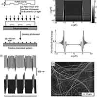
Silicon-on-Insulator Wafers Used for Experimental and computational studies of phase shift lithography with binary elastomeric masks

Research Paper

"First, dry thermal oxidation ͑1100°C, 30 min͒ of a silicon-on-insulator ͑SOI͒ wafer ͑University Wafer; ͗110͘ top silicon orientation with a thickness of 2.5± 0.5 micron, SiO2 with a thickness


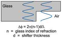
What is Phase Shift Lithography?

A preferred embodiment of phase shift phase shift lithography imagelithography is illustrated in FIG. 25, which is a plan view of a generic phase shift mask blank. The exposure pattern shown in FIGS. 28 and 29 is at right angles to each other and is a double exposure pattern. As an alternative to a single exposure pattern, the method may include a chromeless phase-shift reticle. The features 36 on the photoresist are printed to match the phase-shifting patterns.
 

What is Binary Elastomeric Mask?

A Binary Elastomeric Mask is a flexible polymer layer that is used in conformal binary elastomeric mask diagramcontact with layers of photoresist. The binder is produced by casting prepolymers on a poly(dimethylsiloxane) matrix and then curing the material. The presence of a refractory phase allows the Binary Elastomeric Mask to exploit proximity and near field optical effects.
 

What Are RF Filters?

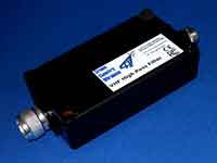
what does an rf filter look likeRF filters are passive coaxial components. They have three basic varieties: linear, nonlinear, and time-invariant. These components allow some frequencies to pass and reject others. Several common frequency bands are covered by different types of RF filters. Among them are WiFi, Bluetooth, GPS L1, and ISM. Several other types are available for specific applications, such as EMI/RFI filters, as well as a range of other less common frequencies.

There are several uses for RF filters, with the list seemingly endless. They provide selectivity in radio receivers by allowing only the appropriate frequency band to pass through. Similarly, they prevent unwanted signals from being transmitted. And they are used to ensure only required mix products are passed on from mixers. For these reasons, they're a crucial component in wireless technology. But how do you know if you need one?

RF filters are crucial in wireless applications. Without them, your application could have a variety of undesirable effects, including interference and reduced range. They could also cause certification failures. Taoglas understands the needs of each project and can develop a filter customized for the specific application. So, what are RF filters? Contact us for more information. And don't forget to check out our RF filters, we'll show you how to choose the best ones for your needs.

An RF filter can be specified in several ways, but its primary use is in reducing unwanted signals. For example, a band pass filter is designed to allow signals of a specific frequency band, while a band reject filter rejects frequencies outside of the pass range. It's typically used on both the transmit and receive path of an RF system. These filters are important in minimizing the bandwidth of the signal, which allows a transmitter to transmit data at the speed it needs.


Video: Basics of RF Filters


What is Optoelectronics?

Optoelectronics is the study of light and electrical energy. This science can be used in a wide variety of what do optoelectronics look likedevices, from traffic lights and LEDs to information displays, optical fiber, and more. The most common devices involving light and electricity are LEDs, photo diodes, and solar cells. The science behind these devices is a vastly fascinating area of study. To learn more about optoelectronics, read on.
Optoelectronics is a rapidly expanding field of science and engineering. Using semiconductor materials to control light, optoelectronic devices are used in electronics. Optoelectronic devices are used for many applications, including telecommunication, monitoring, sensing, medical equipment, and general science. Examples of applications in optoelectronics include solar panels, smart windows, and smart televisions.

Light-based electronics use an optical fibre as a transmission channel. These fibres guide light waves in the optical range. Optical fibres are useful for long-distance communication, as they exhibit total internal reflection. Optical fibres also enable multiplexing signals by wavelength, frequency, or time division. This allows them to transmit different types of information. For example, light-based systems allow for the transmission of a variety of digital signals.

One type of optoelectronics component is a photo-diode. This device is a one-way switch for current, allowing it to flow in one direction while blocking it in the other. Optical fibers, in turn, can be used in telecommunications and consumer electronics. The field of optoelectronics is rapidly evolving. There are countless applications for these devices, including traffic lights, brake lights, and fiber optic communication.


Video: What is Optoelectronic Devices & Applications

Image Sensing in Silicon on Insulator (SII) Wafers and Substrates

The basic components of an image sensor are a two-dimensional array of photodetectors and a readout integrated circuit. Photodetectors are sensitive to incoming light, while the readout circuit quantitatively evaluates the outputs of the detectors and processes them into images. Silicon readout electronics are incompatible with newer detector materials, requiring two separate chips. The two chips are connected by indium bumps bonded to the appropriate nodes of the readout integrated circuit and detectors.

ICS 100 may include an image-sensing device such as a digital camera, medical imaging device, or other device. IC 510 may convert an image into an electronic signal that enables processing and display. This may also comprise the functionality of the IC 100. For example, BSI CIS may provide a higher sensitivity compared to a conventional front-side illuminated image sensor. BSI CIS is also able to capture more photons than a conventional front-side-illuminated image sensor.


Video: Image Sensing and Acquisition

Substrates for Wireless Connectivity

RF devices demand high purity and atomic-scale thickness uniformity. Their frequency response is also influenced by the substrate's sensitivity. As RF components are an integral part of the device, substrates must be co-optimized to achieve the desired frequency response. Wafer and device specifications may vary over time, so design should account for variability among vendors and substrates. Using an engineered substrate for the fabrication of RF components is a cost-effective and convenient alternative.

Various embodiments of the present invention are useful for providing wireless connectivity in a network environment. In one embodiment, the substrate includes electronic circuitry, antenna hardware, and a communication link. The substrate can also be adhered to physical objects and provide enhanced transmission and reception of wireless signals. Further embodiments are discussed below. These substrates may be made of a flexible, transparent material that will not block a window. Suitable substrates include those made of silicone, plastic, or any other material that is flexible.

The most common type of metalink is point-to-point. It implements wireless connectivity over a physical or virtual link. The endpoint sends a Substrate Discovery Message (SDM) to a directly attached substrate router. The substrate router responds by supplying the active terminal with information that allows it to send subsequent control messages. This mechanism enables a host device to maintain a metalink, even while moving from one wireless access point to another.


Video: Substrates for Wireless Connectivity Devices

Flexible Hybrid Electronics

The concept of Flexible Hybrid Electronics (FHE) combines printed, advanced CMOS-based components and a polymeric substrate to form highly efficient, lightweight devices. This technology has great market potential because it offers a range of advantages, including lower cost, improved mechanical flexibility, and improved performance. This new concept provides a comprehensive literature review of FHE development, including its supply chains and design challenges. Read this book to learn about this exciting new technology!

In this paper, two disruptive packaging processes for ultrathin flexible hybrid electronic systems with ICs as thin as 15-20 mm per side are described. The first generation technology is based on a modification of conventional pick-and-place methods and has been demonstrated on a commercial-grade roll-to-roll assembly line with packaging rates of over 10,000 cp/h. The second generation technique involves the integration of multiple technologies into a single packaging process.

The first phase of the development of FHE technology involves a research and development process that can be used in a variety of applications. In the health monitoring field, FHE is proving to be more appealing than other materials. Researchers at Children's Healthcare of Atlanta and NextFlex have developed a wireless wearable monitor. These sensors and the flexible electronics are both transparent and comfortable to wear. Unlike conventional wired sensors, the FHE wires are nearly undetectable by consumers.

The most important segment of Flexible Hybrid Electronics (FHE) is healthcare. It caters to the needs of each person in terms of monitoring, early diagnosis of diseases, and therapy. Wearable electronic devices also gain attention as they can interact seamlessly with the body. They can monitor heart rate, motion, wrist pulse, blood pressure, and even identify intraocular pressure. This advancement is sure to change the way people interact with their environment.


Video: Flexible Hybrid Electronics (FHE) Overview

RF Micro Electro Mechanical Systems

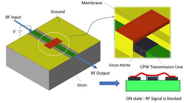
RF MEMS are semiconductor devices that produce radio waves and are widely used in mobile phone applications. These devices use a variety of materials to produce the electromagnetic signals they need. Among the many applications of RF MEMS are smartphones, which automatically adjust the orientation of the screen due to system on a chip technology. Similarly, medical devices, such as disposable pressure sensors, rely on RF MEMS for the production of biosensors.

radio frequency micro-electrical-mechanical systems

RF MEMS can be fabricated using the same fabrication process used in CMOS technology. However, copper passive components have been used in the post-CMOS fabrication of RF MEMS structures. Hence, copper-based devices are a good choice for RF MEMS applications. However, copper is a poor candidate for use in medical applications due to its limited compatibility with other materials. These components must be packaged using hermetic techniques in order to avoid electrical shocks.

As the field of RF MEMS matures, more RF MEMS devices will be developed. The most common devices were developed during the 1990s, thanks to the efforts of researchers at major defense-oriented companies. The Air Force and DARPA funded device-level development efforts. As the technology matured, other Federal services became aware of its potential for improved RF systems. Currently, RF MEMS are being tested for use in terrain-penetrating imaging radar, tunable matching networks, phase shifters, and more.

RF MEMS are monolithically integrated ohmic and capacitive RF switches. As such, RF MEMS represent a viable solution to obtain high linearity, low power dissipation, and high isolation. FBK has developed technology solutions for fully-integrating process fabrication of RF-MEMS switches in CMOS-compatible manufacturing steps. These devices have a long life span and can be used in high-frequency applications, such as telecommunications and GPS systems.


Video: RF MEMS Switch Technology

What is Silicon on Insulator Process?

Silicon on insulator (SOI) is a microelectronic process technology that involves the formation of a thin layer of silicon on top of an insulating layer, typically silicon dioxide (SiO2). The insulating layer is used to isolate the silicon layer from the substrate below, which is typically made of bulk silicon.

There are several benefits to using SOI technology in microelectronic devices. One major advantage is that it allows for improved device performance by reducing parasitic capacitance and resistance, which can lead to faster switching speeds and lower power consumption. SOI technology also allows for the creation of devices with very thin layers of silicon, which can be useful for some applications.

SOI technology is used in a variety of microelectronic devices, including microprocessors, memories, and other integrated circuits. It is also used in sensors, radio frequency (RF) devices, and other types of electronic components.


Silicon on Insulator Radio Frequency (RF) Devices

Silicon on insulator (SOI) technology can be used to create radio frequency (RF) devices, which are electronic components that operate at radio frequencies (typically in the range of 3 kHz to 300 GHz). RF devices are used in a variety of applications, including wireless communication systems, radar systems, and medical imaging.

One benefit of using SOI technology in RF devices is that it can help to improve the performance of the device by reducing parasitic capacitance and resistance, which can lead to faster switching speeds and lower power consumption. SOI technology can also allow for the creation of RF devices with very thin layers of silicon, which can be useful for some applications.

There are several types of RF devices that can be created using SOI technology, including amplifiers, filters, mixers, and oscillators. These devices are used in a variety of different RF systems, such as mobile phones, radios, and satellite communication systems.

Silicon on Insulator (SOI) wafers are used to create a variety of microelectronic devices, including:

Silicon on insulator (SOI) wafers are used to create a variety of microelectronic devices, including:

  1. Microprocessors: SOI technology is used in the manufacturing of microprocessors, which are the central processing units (CPUs) of computers and other electronic devices. SOI microprocessors can offer improved performance and lower power consumption compared to traditional bulk silicon microprocessors.

  2. Memories: SOI technology is used in the manufacturing of various types of memory devices, including dynamic random-access memory (DRAM) and flash memory. SOI memories can offer improved performance and lower power consumption compared to traditional bulk silicon memories.

  3. Integrated circuits: SOI technology is used to create a variety of different types of integrated circuits (ICs), which are devices that contain multiple transistors and other electronic components on a single chip. SOI ICs can offer improved performance and lower power consumption compared to traditional bulk silicon ICs.

  4. Sensors: SOI technology is used in the manufacturing of various types of sensors, including pressure sensors, temperature sensors, and accelerometers. SOI sensors can offer improved sensitivity and accuracy compared to traditional bulk silicon sensors.

  5. Radio frequency (RF) devices: SOI technology is used to create RF devices, which are electronic components that operate at radio frequencies (typically in the range of 3 kHz to 300 GHz). SOI RF devices can offer improved performance and lower power consumption compared to traditional bulk silicon RF devices.

Silicon-on-Insulator Wafers for Photonics Research and Production


Silicon photonics is a technology that involves the use of silicon as the material for creating optical components and devices, such as lasers, modulators, and detectors. These components and devices are used in a variety of applications, including telecommunications, data centers, and biomedical imaging.

One of the key substrates used for silicon photonics is silicon-on-insulator (SOI) wafers. These wafers consist of a thin layer of silicon (typically around 200-300 nm thick) that is grown on top of an insulating layer, typically made of silicon dioxide (SiO2). The insulating layer is then supported by a thicker layer of silicon or another material, known as the substrate.

SOI wafers are useful for silicon photonics because they allow for the creation of devices with very small dimensions, as well as the ability to fabricate multiple devices on a single wafer. The insulating layer also allows for better isolation of the devices from the substrate, which can be important in some applications.

Other substrates that are used in silicon photonics include silicon-on-sapphire (SOS) wafers, which are similar to SOI wafers but with a sapphire substrate instead of silicon, and silicon-on-glass (SOG) wafers, which use a glass substrate. These substrates are used for different applications and have different properties that make them suitable for specific uses.

What Silicon-on-Insulator Spec Is Used to Fabricatate Photonic Integrated Circuits?

For a silicon-on-insulator (SOI) platform that is compatible with microelectronics and suitable for scalable photonic integrated circuits, the following specifications are commonly used:


  • Thickness of the silicon layer: <220 nm (Buy Online!)
  • Thickness of the insulating layer (typically silicon dioxide): <3 um
  • Quality of the insulating layer: high crystal quality, minimal defects
  • Electrical isolation: complete, with low resistance and capacitance


Note that the specific requirements for your application may vary and it is recommended to us for more detailed and tailored advice.

How are soi substrates used to fabricate photonic devices?

Silicon-on-insulator (SOI) substrates are widely used for fabricating photonic devices due to their unique optical and electronic properties. Photonic devices fabricated using SOI include:

  • waveguides
  • modulators
  • filters
  • detectors

Photonic devices manipulate light for various applications in telecommunications, sensing, and computing. The fabrication of photonic devices on SOI substrates typically involves several key steps:

Substrate selection: Choose an appropriate SOI wafer with the desired specifications, including device layer thickness, insulating layer thickness (usually silicon dioxide), and handle layer thickness. The device layer thickness and the optical properties of the insulating layer are crucial for controlling the optical confinement and guiding properties of the photonic devices.


Device design: Design the photonic devices and their layout using computer-aided design (CAD) software. The design should take into account the dimensions, materials, and optical properties required for the specific application.


Lithography: Transfer the photonic device design onto the SOI substrate by patterning a photoresist layer using photolithography. This process involves exposing the photoresist to ultraviolet (UV) light through a photomask that contains the device patterns, followed by developing the photoresist to create the desired patterns on the substrate.


Etching: Remove the exposed silicon material in the device layer to form the photonic structures. This can be done using either wet etching (chemical) or dry etching (plasma). The choice of etching technique depends on the desired device geometry, sidewall profile, and etch rate.

Cladding: Deposit a cladding layer, typically silicon dioxide or other dielectric materials, around the etched photonic structures to provide optical confinement and reduce scattering losses.

Doping and contacts: If the photonic device requires active components, such as modulators or detectors, the silicon layer can be doped to create p-n junctions, and metal contacts can be deposited to facilitate electrical connections.

Packaging and testing: Package the fabricated photonic devices and test their performance in terms of optical properties, such as transmission, reflection, and coupling efficiency.


By leveraging the unique properties of SOI substrates, photonic devices can achieve high levels of integration, low power consumption, and excellent performance, making them suitable for a wide range of applications in communications, sensing, and computing.