Borofloat 33 Wafers to Fabricate Devices
A scientist requested a quote for the following research:
We are looking to fabricate a Silicon-Glass device with Silicon microchannels machines into it before anodic bonding. We plan to use 4 inch silicon wafers (Si, 500 micron thick), and glass wafers thinner than 170 micron so microscopy through it is feasible. Since quality/spec of Si and glass are critical for successful anodic bonding, BF33 wafers I believe are a good choice to start our work with.
- Do you suggest anything different or am I missing anything in terms of materials? In our project, the above device is not the primary focus, so we prefer to optimize on the costs and times.
- Also, in your experience, what would be a good order size (number of wafers) for Si and glass wafers?
UniversityWafer, Inc. Quoted and Sold the following wafer.
BF33 Item #837
100mm 175um DSP Great or anondic bonding, 60/40 scratch/dig
Get Your BF33 Wafer Quote FAST!
Why Use Borofloat 33 Glass Wafers?
Borofloat 33 (BF33) is often chosen by researchers for its durability and resistance to thermal shock. BF33 including silica has very low coefficients of thermal expansion. BF33 has a much higher melting point, over 1500 degrees fahrenheit, than other glass. BF33's is often used in research lab equipment, as well as optical and lighting applications.
Borfloat 33 will break, but it will not shatter. Thus it's easier to handle when there is an accident.
Borfloat 33 hypoallergenic and doesn't contain any lead.
When you need the following properties BF33 is the right choice!
- Outstanding Thermal Resistance
- Exceptional High-Transparency
- High Chemical Durability
- Excellent Mechanical Strength

Custom Borofloat 33 Specification
UniversityWafer, Inc. can customize your wafer specs. 500 micron thickness for 100mm borofloat 33 wafers. Below a client needed BF33 wafers for bonding with the silicon wafer, and the particle size is required to meet the SEMI standard. We provided 400 micron thick glass.
The below glass wafer spec was used for bonding with the silicon wafer, and the particle size is required to meet the SEMI standard.
4 inch glass wafer (BF33) "SCHOTT"
Diameter: 100 mm±0.1,
Thickness: 400±20 μm
Surface Roughness: <1.5nm (Ra)
TTV: <10 μm,
Surface quality 60/40,
Warpage<20 μm,
Chamfered edges, Flat edges
What Kind of Sensors Use Borofloat 33?
Inertial and MEMS Sensors Temperature & Pressure Sensors are jsut some of the sensors that BF33 wafers are great for!
Borofloat 33 Substrate to Fabricate Pressure Sensors
A MEMS researcher requested the following quote:
We have another project that uses pyrex wafers to fabricate pressure sensor. Could you please give us a quotation for:
- 50 pieces of 6" pyrex wafers, double side polished, 500 um thickness.
- 50 pieces of 6" pyrex wafers, double side polished, 700 um thickness.
Because it is very urgent, we are looking forward to hearing from you.
Reference #119319 for specs and pricing.
Five Applications of Borofloat in Aerospace
Borofloat glass is highly valued in the aerospace industry due to its unique properties, such as high thermal resistance, low thermal expansion, and excellent optical clarity. Here are five notable applications of Borofloat glass in aerospace:
-
Space Telescope Lenses and Mirrors: Borofloat glass is used in the lenses and mirrors of space telescopes. Its low thermal expansion and high resistance to thermal shock ensure that these components maintain their shape and alignment in the extreme temperature variations of space. This stability is crucial for capturing high-resolution, distortion-free images of celestial bodies.
-
Aircraft and Spacecraft Windows: In aircraft and spacecraft, windows need to withstand significant pressure differences and temperature extremes while providing clear visibility. Borofloat glass, with its high mechanical strength and thermal resistance, is an excellent material for such applications. It ensures the integrity and safety of windows in these high-stress environments, while also offering clarity and resistance to scratching and impact.
-
Instrumentation Panels and Displays: The durability and optical clarity of Borofloat glass make it ideal for use in the instrumentation panels and display screens in both aircraft and spacecraft. These panels need to remain clear and readable in various conditions, including exposure to UV radiation, extreme temperatures, and potential chemical interactions. Borofloat glass can endure these conditions without degrading.
-
Optical Components for Sensors and Cameras: Aerospace applications often require high-precision optical components for sensors and cameras, which are used for navigation, observation, and data collection. Borofloat glass is used in these components due to its excellent light transmission properties, low fluorescence, and stability under temperature changes and radiation exposure common in space environments.
-
Lighting Systems: In aerospace, lighting systems need to be reliable, efficient, and resistant to extreme conditions. Borofloat glass is used in the covers and lenses of these lighting systems due to its high thermal resistance and strength. It can withstand the heat generated by lighting systems and protect sensitive components from harsh environmental conditions.
Overall, Borofloat glass's combination of thermal stability, optical clarity, and mechanical strength makes it an invaluable material in the aerospace industry, significantly contributing to the safety, efficiency, and effectiveness of various aerospace applications.
What are Borofloat's Low Thermal Expansion Benefit Micoelectronics?
Borofloat glass's low thermal expansion is particularly beneficial in the field of microelectronics for several reasons:
-
Thermal Stability in Component Manufacturing: During the manufacturing process of microelectronic components, materials are often subjected to high temperatures. Borofloat glass, with its low thermal expansion, remains dimensionally stable under these conditions. This stability is crucial for maintaining the precision and alignment of intricate microelectronic components.
-
Substrate Material for Thin-Film Deposition: In microelectronics, thin films of various materials are often deposited on substrates. Borofloat glass, due to its low thermal expansion, provides an ideal base for these thin films. It minimizes the risk of warping or cracking that can occur if the substrate expands or contracts differently from the thin film, thereby ensuring the integrity of the microelectronic devices.
-
Reduced Stress on Integrated Circuits: Integrated circuits (ICs) are sensitive to thermal stress, which can cause failure or reduce performance. Since Borofloat glass expands and contracts very little with temperature changes, it minimizes the stress on ICs mounted on it. This is particularly important in applications where ICs are exposed to fluctuating temperatures.
-
Improved Heat Management: Effective heat management is crucial in microelectronics to prevent overheating and ensure reliable performance. The thermal stability of Borofloat glass makes it an excellent choice for applications like heat spreaders or cooling substrates, helping to evenly distribute and dissipate heat generated by electronic components.
-
Enhanced Reliability and Longevity: The low thermal expansion of Borofloat glass contributes to the overall reliability and longevity of electronic devices. By reducing the mechanical stress caused by thermal expansion, it helps prevent cracking, warping, or delamination of components, which can lead to device failure.
In summary, Borofloat glass's low thermal expansion is highly advantageous in microelectronics manufacturing and design. It contributes to the production of more reliable, stable, and long-lasting electronic devices by mitigating the effects of temperature variations on materials and components.
How is Borofloat Used in Solar Windows?
Borofloat glass plays a significant role in the development and efficiency of solar windows, a technology that combines the functionality of traditional windows with the ability to generate solar energy. Here's how Borofloat is used in this context:
-
Durability and Weather Resistance: Solar windows must withstand a variety of environmental conditions including temperature fluctuations, UV exposure, and physical impacts. Borofloat glass is highly resistant to thermal stress and chemical corrosion, making it an ideal choice for solar windows that are exposed to the elements.
-
High Optical Clarity: For solar windows to be effective, they must allow light to pass through while also harnessing it for energy production. Borofloat glass offers excellent light transmission across a wide range of wavelengths, which is essential for both visibility through the window and optimal performance of the photovoltaic (PV) cells integrated within the window.
-
Thermal Management: In solar window applications, managing the heat generated by PV cells is crucial to maintain efficiency and prevent damage. The low thermal expansion coefficient of Borofloat glass helps in reducing the stress on the PV cells caused by thermal expansion, thereby enhancing the longevity and performance of the solar windows.
-
Integration with Photovoltaic Materials: Borofloat glass is compatible with various photovoltaic materials and technologies. It can be used as a substrate for thin-film solar cells or as a protective cover glass for crystalline silicon cells and other types of solar modules integrated into windows.
-
Aesthetic Flexibility: Solar windows often need to be aesthetically pleasing, especially when used in residential or commercial buildings. Borofloat glass can be easily tailored in terms of size, shape, and surface finishing, allowing for greater flexibility in design and architecture.
-
Energy Efficiency: By combining the functions of a window and a solar panel, Borofloat-equipped solar windows contribute to the energy efficiency of buildings. They provide natural light while generating renewable energy, reducing the overall energy consumption and carbon footprint of the building.
In summary, Borofloat glass enhances the functionality of solar windows through its durability, optical clarity, thermal management properties, compatibility with PV materials, aesthetic versatility, and contribution to energy efficiency. This makes it a key component in the advancement of solar energy technologies integrated into building designs.
How DoesBorofloat's Benefit The Medical Industry?
Borofloat glass, with its unique combination of chemical resistance, high light transmission, low fluorescence, and excellent flatness, offers several significant benefits to the medical industry:
-
Chemical Resistance for Sterile Environments: In medical settings, materials must withstand rigorous sterilization processes often involving harsh chemicals and high temperatures. Borofloat glass's high chemical resistance ensures it can endure these conditions without degrading. This makes it ideal for use in medical devices and laboratory equipment that require regular sterilization to maintain a sterile environment.
-
High Light Transmission in Diagnostic Equipment: The clarity and high light transmission properties of Borofloat glass are essential in various diagnostic equipment, such as microscopes and imaging devices. These applications require a material that allows for clear, unobstructed observation and precise image capture. The high optical quality of Borofloat glass ensures accurate and reliable results in medical diagnoses.
-
Low Fluorescence for Accurate Analysis: In fluorescence microscopy and other applications where fluorescent labeling is used for analysis, low fluorescence is crucial. Borofloat glass exhibits low inherent fluorescence, reducing background noise in fluorescent imaging. This leads to more accurate and clearer images, which is vital for detailed cellular and molecular studies.
-
Excellent Flatness for Precision Instruments: The exceptional flatness of Borofloat glass is beneficial in the production of precision instruments such as slides and coverslips used in microscopy. This flatness is critical for ensuring consistent focus and image clarity across the entire field of view, which is essential for detailed medical analysis and research.
-
Durability in Harsh Environments: Medical environments can be demanding, with equipment often exposed to extreme conditions. Borofloat glass's durability makes it suitable for use in such environments, ensuring the longevity and reliability of medical instruments and devices.
-
Bio-compatibility: For medical applications that involve direct contact with the human body, such as in certain implantable devices, the bio-compatibility of Borofloat glass is a significant advantage. Its inert nature reduces the risk of adverse reactions, making it safe for use in a variety of medical implants and devices.
-
Versatility in Medical Device Fabrication: Borofloat glass can be precisely cut, shaped, and finished to meet the specific requirements of various medical devices. This versatility allows for its use in a wide range of applications, from laboratory slides to complex components in medical machinery.
In summary, the unique properties of Borofloat glass, such as chemical resistance, high optical transmission, low fluorescence, and excellent flatness, make it a valuable material in the medical industry. It contributes to the accuracy, reliability, and safety of medical diagnostics, research, and treatments.
How Does Borofloat's Clarity and Thermal Stability Benefit Optical Devices?
Borofloat glass's exceptional clarity and thermal stability offer significant benefits to optical devices in several ways:
-
High Optical Clarity for Improved Imaging Quality: The outstanding clarity of Borofloat glass allows for unimpeded transmission of light, which is crucial for the performance of optical devices like lenses, prisms, and windows. This high degree of transparency ensures that images are bright and clear, enhancing the overall quality of optical imaging.
-
Thermal Stability for Dimensional Consistency: Optical devices often operate under varying thermal conditions. Borofloat glass's high thermal stability means that it undergoes minimal expansion or contraction with temperature changes. This dimensional consistency is vital for maintaining the precise alignment of optical components, which is essential for accurate imaging and measurement.
-
Resistance to Thermal Shock: In situations where optical devices are subject to rapid temperature changes, the resistance of Borofloat glass to thermal shock prevents cracking or breaking. This property is particularly important in applications like astronomical telescopes, where night-time cooling can be rapid, or in industrial optical systems exposed to high-intensity light sources.
-
Durability in Harsh Environments: The robustness of Borofloat glass against physical and chemical stressors ensures the longevity and reliability of optical devices, even in harsh environments. This durability is critical for maintaining the performance of precision optical instruments in industrial, scientific, and outdoor settings.
-
Consistent Optical Properties Over a Wide Temperature Range: Borofloat glass maintains its optical properties across a broad temperature spectrum. This consistency ensures reliable performance of optical devices in applications that involve extreme or fluctuating temperatures, such as in space exploration or high-temperature industrial processes.
-
Compatibility with Precision Coatings: Optical devices often require specialized coatings for functions like anti-reflection, filtering, or enhancing light transmission. The surface properties of Borofloat glass make it highly compatible with such coatings, ensuring that they adhere well and perform as intended.
-
Reduced Stress on Optical Assemblies: The low thermal expansion of Borofloat glass minimizes stress on optical assemblies caused by thermal expansion mismatches between different materials. This reduced stress is crucial for maintaining the structural integrity and alignment of complex optical systems.
In summary, the clarity and thermal stability of Borofloat glass make it an ideal material for a wide range of optical devices. These properties enhance the performance, durability, and reliability of optical systems in various applications, from precision scientific instruments to everyday optical tools.
Borofloat 33 (BF33) - Borosilicate Float Glass from SCHOTT
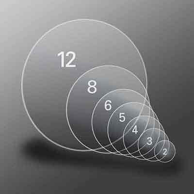
We have a large selection of Borofloat 33 glass wafers in all sizes. We have borofloat as thin as 100 microns. Borofloat 33 is the sanme as Pyrex 7740 and have the same anondic bonding properties. Diameters range from smalled diced pieces up to 12 inches.
BUY ONLINE HERE!
BOROFLOAT® 33 is a high quality boro-silicate glass with outstanding properties for a wide-range of applications.
This unique special float glass is manu-factured by SCHOTT JENAer GLAS using the Microfloat process and the latest technology. This technology also results in a homogeneous material that has an excellent mirror-like surface, a high degree of flatness and an outstanding optical quality.
BOROFLOAT® 33 is a clear and transpar-ent colourless glass. Its excellent trans-mission and its very weak fluorescence intensities over the entire light spectrum make BOROFLOAT® 33 ideal for a wide range of applications in optics, optoelec-tronics, photonics and analytical equip-ment.
Its low thermal expansion, its high thermal shock resistance and its ability to withstand temperatures up to 450°C for long periods make BOROFLOAT® 33 a good choice for applications which call for good temperature stability (e.g. internal panels in pyrolytic self-cleaning ovens and over plates for high-power floodlights).
BOROFLOAT® 33 is highly resistant to attack by water, strong acids, alkalis as well as organic substances. Therefore it is particularly suitable for applications in the chemical industry such as sight glas-ses for reaction vessels and fittings.
Another interesting field of application is in medical and analytical technology. Measurements are hardly influenced by the glass receptacle because the expo-sure to water and acids results only in the leaching out of small amounts of ions from the glass.
BOROFLOAT® 33 has a lower density than soda lime float glass. It makes it possible to construct lightweight lamina-ted glass systems (e.g. bulletproof glass).
BOROFLOAT® 33 has proven itself in many traditional applications and, today, there is an increasing area of usage in new and technically sophisticated special glass applications such as biotechnology, microelectronics and photovoltaics.
Borofloat 33 Applications
• Home Appliances (interior oven doors, fittings in microwave appliances, window panels for fireplaces)
• Environmental engineering, chemical industry (resistant linings and sight glasses for reaction vessels, microfluidic systems)
• Lighting (protective panels for spotlights and high-power floodlights)
• Photovoltaics (glass for solar collectors)
• Precision engineering, optics (optical filters and mirrors etc.)
• Medical technology, biotechnology (slides, biochips, titration plates, DNA sequencers, microfluidic systems)
• Semiconductor engineering, electronics, sensors (wafers, display glass)
Specification sheet available upon request!
UniversityWafer Borofloat33 and Fused Silica Glass Used for Thin Film Solar Cell Applications
Researchers from the Middle East Technical University and the University of Washington-Seattle have used our 1.1 mm Borofloat33 glass and fused silica glass. These glass items were coated with aluminum by thermal evaporation and annealed at 600 degrees Celsius for 1 hour.
ABSTRACT: Texturing of glass substrate is an alternative novel method for light trapping, which to enhance the
absorbed light by way of increasing the diffused transmittance (haze) so that the amount of absorbed light will be
increased instead of texturing transparent conductive oxide (TCO). In this study, aluminum induced texturing (AIT)
technique is used to texture different type of glasses to see the effect of the chemical composition on surface
morphology and optical properties. Improvement in haze values as well as total transmission were obtained in all
cases subsequent to texturing. High haze values are obtained by additionally enhancement in total transmission.
Surface morphological characterization showed that the composition of glass have direct effect on the textured
profile. We speculate that the components of glass other than SiO2 is affecting the density of reaction starting point
densities initiation cites on the glass-Al interface.
Keywords: Aluminum Induced Texturing (AIT), thin film solar cell, haze...
Research
How do I Bond Wafers Using Borofloat 33 Glass?
Researcher:
I need to bond two glass wafers together for my PhD, on one of which there will be a SiO2 layer with some couple hundred nanometer deep features etched in or deposited using liftoff. However, I am facing great difficulty bonding my glass to one another. Even just at the point of the initial bonding and I believe that the glass I am currently using (one polished 1.1mm thick 1 inch square for one substrate and a nondescript 24x24mm square cover slip as the other substrate) is not flat enough, as I am not able whatsoever to get these substrates to even get to initial bonding. I'm pretty sure my cleaning procedure and our clean room facility are adequate to eliminate particle contamination as the culprit, so I have the suspicion that the surface roughness and flatness of the glass I am using is insufficient. I want to experiment with well known flat glass wafers which are used for anodic bonding and see whether these would help. I saw that the wafers with ID 1837 are marked as good for anodic bonding, however they have a 5 week lead time and are probably too thick to use with a x100 objective. Could you advise me on alternative wafers that are similar and are in stock?
UniversityWafer, Inc. Quoted and Client Purchased:
BF33 Item #1837
100 mm dia. X .175 mm 60/40 S/D
What Borofloat 33 Wafers are Commonly Used to Research Microfluidic Devices?
Researcher:
I was looking at Silicon wafers and Borofloat 33 glass wafers. Probably the 100mm sizes. Wondering if you have any considerations for the specs on the different polishes and such. Application is a microfluidic device of porous media. I am wondering if I need to consider certain grades and such rather than just the standard. I am just looking at the standard ones right now. It would be to make a microfluidic flow cell of porous media where a dry etched (DRIE) silicon wafer is bonded to a glass wafer (anodic bonding.) The resolution won't be too high as it will be with a soft photomask. I can figure it out myself if needed just wondering if you had any recommendations.
UniversityWafer, Inc. Quoted:
100mm BF33 500um DSP 60/40 Scratch/Dig
150mm Borofloat 33 Glass Substrates to Etch Channels in Silicon
Microfluidic device research: Silicon wafer used to etch channels into,
Borofloat wafers to be bonded on top to form capping layer for device.
Researcher purchased:
6inch silicon wafers, 375+/-25um thickness and doubled sided polished, P-type Boron. doped, Resis. 1~100 Ohm.cm,<100> orientation.
and
Item 3867: Borofloat 33 Glass 150mm DSP 1100um Ground Edges
What Borofloat 33 Wafers Are Used to Research Colloidal Linkages?
Borosilicate glass (BF33) have been used to research Brownian lithographic polymers of steric lock-and-key colloidal linkages by scientists at UCLA.
BF33 Item #517 - 100mm 500um DSP Scratch/Dig 60/40 - Price depends on quantity. Buy as few as one wafer!
Research Paper
What Are Brownian Lithographic Polymers?
What are Brownian lithographic polymers? The term refers to the polymers that are manufactured by a process that allows them to form preassembled structures. However, unlike colloidal materials, polylithomers are not created through programmable molecular attraction. Instead, they form as a result of conformational fluctuations caused by brownian excitations. Interconnected colloidal structures can be considered to be miniature models of polymers, whereas they are simply Brownian systems of colloidal linkages.
Various techniques, including lock-and-key particle tracking and lithographic preassembly, are used to determine whether these materials are suitable for immersion lithography. These methods use the properties of these polymers to produce the structures they need for a given application. Because they use Brownian excitations, they provide the flexibility and entropy that a photovoltaic process cannot.
The two basic types of PLMs are symmetric and multiheaded. The former has three pairs of symmetric side chains off its central backbone. The latter, meanwhile, is known as a multiheaded branching LM. It is difficult to create a monomer with this structure, due to practical reasons. It is also possible to produce PLMs with a much smaller size than a typical lithographic process.
PLMs are a special type of polymer that has substantial extensibility. This is particularly interesting in 2D systems where asymmetric interactions among noninterlocking particles can result in Mermin-Wagner fluctuations. Furthermore, an expanded quasicrystal, called a pentatic liquid, can influence the Kosterlitz-Thouless phenomenon and Goldstone modes. This type of lithographic material makes dense, mobile two-dimensional Brownian systems a viable option.
What Borofloat 33 Wafers Are Used for Flexible Transparent Conductive Electrodes Research?
In 2017, scientists from The National University of Ireland and Tyndall National Institute purchased the following borofloat 33 (BF33) wafers for their flexible transparent conductive electrodes research.
BF33 Item #517
100mm 500um DSP 60/40
The Research can be found here.
What Borofloat Wafer Spec is Used for Microfluidic Surface‐Enhanced Raman Spectroscopy Immunoassay?
Scientists have used our BF33 Item #517 - 100mm 500um DSP for their cancer research.


