Glass Wafers BK7, BF33, D263, Corning Eagle, Soda Lime
Which Glass Wafers are Used to Fabricate Microstructures?
A visiting scholar at a major US university was researching microstructures using glass wafers. The researcher was unsure which glass wafer he should use. We helped him with the specs and provided the best price for the quantity desired with fast lead-times.
"We would like to order some glass wafers as our
microfluidic chip ubstrate. We
will pattern some micro-scale
golden wires with on the
substrate surface, which will
be sealed by PDMS topping. The thickness similar to the normal microscope glass slide should
be good enough.
Do you have any recommendation
of 4-inch or 5-inch glass wafer
(with price)?"
Please reference # for specs and pricing. Or buy as few as one wafer online!
Get your quote today and start researching!
Soda Lime Wafers
Applications:
- Where too much heat build up is a problem
- Hot mirrors to reflect Infrared and Transmitting Visible Light
- Cold mirrors for trasmitting Infrared (IR) and Reflecing Visible Light
D 263 Wafers
Applications:
- Touch Control Panels
- Liquid crystal Displays
- Electroluminescent Displays
- Solar Cells
There are several types of diameter of 100 mm glass wafer: ID 518, 540, 1943, 1945, 1950, and 3499. They are in different thickness, surface features and prices. For my use, a thickness of 500 mm is Okay, thus ID 518, 540 may be more favorable. I want to inquire that which is difference the two. In my project, the surface of the glass wafer should be as flat as possible, because we need to spin coat photoresist for photolithography. Item#518 Item# 540 Item# 1943 Item# 1945 Item# 1950 Item# 3499.
The suggest the following fused silica item that the client purchased.
100mm 500um DSP Fused Silica JGS2 1 Flat Primary Flat 32.5+/-2mm, Top Side Ra <10A, S/D 40/20
What Glass Wafers Do I use for a Backplane for PDMS Stamps
Research scientists have used the following glass specs for their PDMS stamps.
D263 or Soda Lime Glass
5.118” square
.022” thick
Please let us know which dimensions you can use for an immediate quote.
What applications use Glass Wafers
D263 glass is great for computer, phone high resolution display technology and production. Thin D263 glass panes are also used for lenses, which is often more expensive than the cost of a conventional glass lens.
D263 is also used in mechanical polishing treatments and to manufacture microelectromechanical systems (MEMS) on different substrates. D263 glass wafers are fantastic for the production of high-performance, cost-effective and flexible microprocessors, meeting the high performance and low cost requirements of a wide range of applications
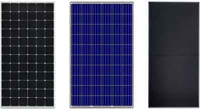
Glass Wafer Solar Cell Cover
When it comes to protecting your photovoltaic cells, the most common and cost-effective choice is a glass  wafer solar cell cover. This type of cover consists of two parts: a backsheet made of ultra-durable plastic, and a thin glass sheet that filters the sun's light into the solar cells. A glue called ethylene vinyl acetate holds the various parts together. The metal frame that encloses the solar cells latches onto the mounting clamps on your roof.
 In order to create solar cells, a thin sheet of glass is pressed onto a metal frame. The metal frame protects the solar panel against inclement weather, and helps to align it at the desired angle. The glass sheet protects the solar cells by blocking out all sunlight except for the solar panel's surface. While the glass wafer is a great choice for protection, it's important to remember that it's a slew of other materials, including aluminum, that can cause arcing and reduce optical transmission.
When it comes to solar cells, glass wafer solar cell covers can help protect the solar cells from damage. They prevent sunlight from leaking into the cell. These covers are usually made from high-quality polymers. For instance, those made from D263 glass can last for many years. And while the glass may not look pretty, it's far more durable than its plastic counterpart. And the added protection of the glass wafer solar cell cover will protect your solar cells against the weather.
Soda Lime Glass Wafer Microslides
The chemical composition of Glass Wafer Microslides varies. The most common ones include 3-aminopropyltriethoxysilane, a compound with a NH2 group that attracts hematoxylin but does not adhere to it. Depending on the type of slide, a different percentage of silane will be used to coat it. This method is the best for creating uniform layers on the glass slides.
The manufacturing process for Glass Wafer Microslides starts with sand, limestone, soda, and chemicals.  This material is heated to 1700 C or more than 3000 F, and then poured onto a thin layer of tin. This process has been used for centuries, and glass slides have been discovered when volcanoes erupted. It can last for years and is considered the best option for research in many fields.
Glass Wafer Microslides are manufactured using different materials. For example, borosilicate glass is one of the cheapest materials to use in glass fabrication. Soda lime glass, on the other hand, is commonly used for mirrors and microslides. Soda lime is a common type of glass for glass slides. It has a low density and high chemical resistance. Borofloat is a floatable borosilicate material.
Using proprietary technologies, Swift Glass manufactures its glass wafer microslides for a variety of industries. The wafers are carefully shaped before being subjected to a controlled inspection process. Precision laser measuring equipment is used to measure the variation in thickness and shape of each GlassWafer. The final product is thoroughly examined. The manufacturer of these products uses sophisticated optical and mechanical techniques to ensure the highest quality.
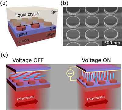
Glass Wafers for Liquid Crysal Displays
![]() Glass Wafers for Liquid Craysal Displays are manufactured by coating silicon wafers with a polymer. This enables the liquid crystals to align with the glass's surface. The most common agents are polyvinyl alcohol, some silanes, and a mixture of these. A semi-dry process provides the best throughput, while a wet process provides a thin, uniform coating.
Glass Wafers for Liquid Craysal Displays are manufactured by coating silicon wafers with a polymer. This enables the liquid crystals to align with the glass's surface. The most common agents are polyvinyl alcohol, some silanes, and a mixture of these. A semi-dry process provides the best throughput, while a wet process provides a thin, uniform coating.
The process of making Glass Wafers for Liquid Cryl Displays begins with the production of a silicon wafer.  The glass and silicon wafers are laminated together using a perimeter seal. The individual display dies are then separated from the laminate by a singulation process. This process may be mechanical, laser scribing, or sawing. The former is preferable, since it preserves the conductors on the inner surfaces of the stacked LCD. In addition, a partial sawing process is preferred to prevent the leakage of cooling fluid into the cell.
The glass and silicon wafers are laminated together by a perimeter seal. After assembling the two substrates, a singulation process separates individual display dies from the wafer laminate. This process can be mechanical, by laser scribing, or by dicing with a saw. The singulation process must only affect the outer surface of the laminate. The inner surface of the glass substrate must remain intact.
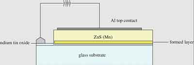
Glass Wafers for Electroluminescent Display
 For the manufacture of an ELED, glass wafers are used. These cylindrical pieces of precision glass are used in a variety of technical and industrial applications. Swift Glass' proprietary glass fabrication processes allow for precision machining, lapping, and inspection. These wafers are subjected to a rigorous, highly controlled quality inspection process. High-precision laser measuring equipment measures thickness variations. Once the finished product is inspected, it is packaged and shipped.
Besides being used for LED, electroluminescent display, and MEMS technology, glass wafers are also used  in a range of integrated circuit packaging applications. In this type of packaging, the glass acts as the substrate and provides improved stiffness and roughness. It also helps protect IC from impact, corrosion, and impacts. The glass is a good carrier for contract pins, leads, and traces. Regardless of the application, glass wafers are an ideal choice for manufacturers of these products.
 These glass wafers are made from sheet glass. The thin panes of D263 glass panes are ideal for high resolution display technologies. They are also more expensive than conventional glass lens, but they are better for the consumer. For example, researchers at Duke University recently bought 25 mm x 50 mm silicon wafers with a thickness of 0.13 mm. The silicon wafers were then used to study sequential biocidal activity and were packaged in coverslips at the University of Wafer.
UniversityWafer Silicon Wafers Used Research on Nanopatterned Antimicrobial Enzymatic Surfaces
Researchers from Duke University purchased 25 mm x 50 mm silicon wafers with a thickness of 0.13 mm for the purpose of studying the sequential biocidal activity and fouling-release of SEM.
Silicon wafers and glass coverslips (size=25 × 50 mm, thickness=0.13 mm) were purchased from University Wafer.
Preparation of a macroscopically patterned surfaces To examine the adsorption of lysozyme under conditions similar to those employed for backfilling, we prepared a sample in which half of the surface was degraded initiator and half was unpatterned PNIPAAm as shown in Scheme S1.

What Are the Electronic Devices Made of Glass?
Glass is the most common material for electronic devices. Its sturdiness and low cost make it a good choice for many applications. With its unique physical and electromagnetic properties, it offers many advantages over other materials. Some of these benefits include increased energy efficiency, reduced cost, and improved performance. These benefits make it an attractive replacement for plastic in many products. But do you need to use glass in your electronics?
The most common form of glass is borosilicate glass. It is made by melting certain substances and producing a glass with a high degree of purity. Its composition includes silica sand, borosilicate, potassium oxide, zinc oxide, and trace amounts of aluminium and calcium oxide. These properties make it ideal for use in electronics. As you can see, a glass device can be used in a variety of ways.
Glass is not only a popular material for electronics, but also for many other applications. It can be used to build high-end buildings, windows, and windshields, and it is a versatile material. This versatility makes it the perfect choice for electronic devices, whether they are made of semiconductors, batteries, or other materials. It is a highly affordable material, and it can also be used for a variety of other applications.
Glass has many uses in electronics. It is one of the most commonly used materials in laptops, mobile phones, and other portable devices. The material is lightweight and durable, and it can handle extreme weather conditions. It is chemically resistant and recyclable, and it is highly resistant to many types of substances. As a result, glass is an excellent choice for electronic devices. It also contributes to the growth of the electronics industry as it develops new technologies.
Glass is used in many different types of electronic devices. Most commonly, this material is used in laptops, televisions, and other portable gadgets. But it is not only limited to these uses. It is also used in medical products, such as for medical purposes. It can also be found in kitchen appliances, furniture, and other items. In addition to its durability, glass is also used in consumer electronics. What are the electrical devices made of glass?
Glass is used in virtually all electronic devices. It is also used for pharmaceuticals, computers, and electronics. As its use grows, it is also used in medicine and in the construction of medical devices. In fact, the glass industry is a huge industry in the U.S. because it is widely available. In fact, it is used in everything from refrigerators to mobile phones. The technology in electronic glass is unimaginable without it.
The most common type of glass is alkali-aluminosilicate. This is the most common type of glass used in portable electronic devices. It is also used in home appliances. However, there are other types of glass. Some are made of alkali-aluminosilic sheet glass. But it is also used in refrigerators. If you're interested in learning more about this material, consider taking a look at its properties and how it can be used for electronic devices.
Alkali-aluminosilicate sheet glass is the most commonly used for cell phones. It is also used for computer screens and other portable electronic devices. It is also used for televisions and other home electronics. There are many other types of glass. For example, borosilicate glass is widely used in smartphones. But it is not always the most common type of glass. It is used for many different applications.
Alkali-aluminosilicate sheet glass is used in most portable electronic devices. It is also used in the windows of houses and cars. It is also used in kitchenware, bottles, and jars. There are several types of glass. Some of them are aluminosilicate glass, while others are borosilicate glass. Both types of glass are used for making portable electronic devices.
What Glass Wafers Used for Integrated Microsystem for Dielectrophoretic Cell Concentration and Genetic Detection
Device design and fabrication
The mask design for the microsystem is presented in Fig. 1.
Two independent inlet channels connect through a series of
PDMS microvalves to a common central cell capture channel.
The cell capture channel (167 mm wide, 100 nL in volume)
contains a set of interdigitated electrodes (20 mm width, 20 mm
spacing), which are powered with AC frequencies to establish a
dielectrophoretic force on bacteria in the sample stream.
Filtered sample passes through a PDMS microvalve at the end of the capture channel to waste. The microvalves are similar to
those described by Grover et al.17 The dead volumes of these
microvalves are 50 nL each.
To form the microchannels, a 0.55 mm thick, 100 mm
diameter glass wafer (University Wafers, South Boston, MA) was cleaned and a 200 A°
layer of chrome was deposited on one
side using electron beam evaporation. The chrome was used
to form a reflective surface for optical alignment of both substrates during the flip-chip bonding process.
To form the electrodes, a 100 mm diameter glass wafer (0.55 mm-thick, University Wafers, South Boston, MA) was cleaned and photoresist was spun on and photolithographically patterned. Following deposition of 200 A° of Ti and 2000 A° of Pt using electron-beam evaporation, standard liftoff was performed by sonicating the wafer in acetone for 10 min.
Please contact us for the type of glass another other specs!
