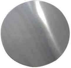
I'm looking for 6 in (150mm) Aluminum dummy wafer as a carrier substrate for a proprietary CVD process. How polished is the surface? What are the cost of bare vs anodized?
Aluminum Wafers are a Great Silicon Replacement
What are Aluminum Dummy Wafers Used For?
A senior research and development scientist use Al substrates as carriers and requested the following quote:
Reference #279485 for specs and pricing.
Get Your Quote FAST! Or, Buy Online and Start Researching today!
Aluminum substrates are materials used as the base or foundation for various types of products, such as printed circuit boards (PCBs), thin-film solar cells, and LEDs. The use of aluminum as a substrate material offers several advantages, including good electrical and thermal conductivity, high strength, and low weight. Aluminum substrates are often used in the electronics industry because they can help to improve the performance and reliability of electronic devices. They are also used in the aerospace and automotive industries because of their low weight and high strength.
 We have a large selection on Aluminum discs available in all diameters, thicknesses and quantities.
Do you Guys Make Aluminum Substrates?
Scientist Asks:
We would like to coat Boron-10 on 0.25 mm thick and 4” diameter or bigger? Aluminum substrate.
We provided:
Diameter 4 inch
Thickness 0.3mm SSP
Do you offer any Aluminum-Coated 4-inch Silicon Wafers?
We’re looking for 10 nm Ti + 100 nm Al, or something comparable. We just need the top layer to be Al. Initially we’d like a quantity of about 20.
We quoted:
100mm P/B (100) 500um Al/Ti SSP 8-12 ohm-cm SEMI Prime, 2Flats, PF@<100>±1°, SF 45° CW from PF, with 10nm barrier layer of Ti & 100nm±5% layer of Al on polished side only, in Empak cst
Above we offer Silicon wafers with 100nm layer of pure Aluminium over the polished side.
We can also offer a layer of 99.5%Al 0.5%Cu or 98%Al 2.0%Cu in place of 100%Al, at the same price.
In the past you have been able to supply us with aluminized silicon wafers
Im hoping you can do that for us again. Here are the specs:
Required:
Diameter: 25.4mm diameter, +0, -150 microns
Aluminum on ONE polished surface, thickness >=50 nm.
Preferences:
No flat is GREATLY preferred
Orientation: <100>
Dopant: undoped, but no real requirement
Preferably DSP
Thickness: <300 microns, 280 micron preferred.
Resistivity: <10,000 ohm-cm
Well order at least 25 units.
I am looking for aluminum wafers, 3" and 4" , DSP, 0.5 mm and thicker, 5 pcs of each. Can you help?
We sold
3" SSP 0.5 mm and thicker
4" SSP 0.5 mm and thicker
Buy Aluminum Online and Save!
We have a large selection of Al wafers for all your needs.
A researcher need our Al.
We need 30 high purity aluminum disks with single side polished for a project. My colleague recommended  me to check with . The dimensions needed are: 25.4-mm in diameter and 1.75-mm in thickness. Could you please make this for us? If yes, could you please let me know the estimated cost? And turnaround time?
The disks will be used for electroplating, so we will need flatness tolerance of the polished side to be better than 0.005 mm. And we need 0.05 mm tolerance for the diameter and 0.02 mm tolerance for the thickness 99.99% pure.
Advantages of Aluminum Wafers
Aluminum wafers l can be used for a variety of applications, including solar cells, semiconductor chips, and other electronic devices. Aluminum wafers are highly durable and shatterproof. Their high density makes them the best choice for semiconductors. Moreover, they meet the requirements of the semiconductor industry. They are easy to handle and can be packaged without affecting the shape or the quality of finished products. In addition, they are shatterproof. As a result, they are suitable for a wide variety of applications. If you need a high-quality, durable material, aluminum wafers are the best choice.
Aluminum wafers can be produced in a wide variety of shapes and sizes. Regardless of their shape, they are shatterproof. They also meet the requirements of semiconductor manufacturing. For example, you can produce thin-film transistors and high-speed computer chips with an aluminum alloy plate. You can also create other types of materials with these materials. You will find it hard to choose one that will satisfy your needs.
The density of aluminum wafers is the highest of all. Standard sizes are 25 mm (1 inch) in diameter. They are produced through ultra-high purification techniques. A customized composition can be created with the company's custom production capabilities. In addition, aluminum wafers are available in various forms and shapes. In addition to wafers, American Elements also produces copper and nickel-based films, nanoparticles, solutions, and organometallics.
UniversityWafer, Inc. and our partners can fabricate Aluminum Wafers in standard sizes. Their standard sizes range from 25.4 mm (1 inch) to 300 mm (11.8 inches). The company also produces custom compositions. These include nanoparticles, solutions, and organometallics. These materials are used in a wide variety of industries. However, the most common applications for aluminum wafers are in the semiconductor industry. Its density is essential for making semiconductors.
Aluminum Substrates for Semiconductor Applications
Aluminum substrates for semiconductor applications have a variety of uses. They can be used for thin-film substrates, power diodes, or even lattice strain applications.
![]()
Power diodes
Power diodes are semiconductor applications in which a large amount of current flows unidirectionally through the device. They are used in voltage regulation and surge protection. They are widely used in a wide range of electronic devices.
A wide variety of materials have been used for printed diodes. These include silicon, metal oxides, organics, and even nanomaterials. Each of these materials has a unique set of properties. However, the best material combinations are still not well understood. Hence, future development may depend on the introduction of new materials.
The most promising candidates for printing are organic materials. These have a very low cost and high uniformity. Moreover, these are highly compatible with printing fabrication methods. Nevertheless, organics suffer from certain material limitations. This is especially true for HF (high frequency) applications, where the resistance of the metal and semiconductor should be kept as low as possible.
The optimum combination of materials for a diode is not clear yet. However, nanomaterials have shown the highest electrical performance. Their superior flexibility and charge carrier mobilities make them ideal for flexible semiconducting applications. They are also solution processing friendly.
Although the material limitations of organic materials are often an impediment to the development of these diodes, their potential as high-performance, low-cost electronic components is promising. In addition, the fabrication process for these organic diodes is close to maturity. Consequently, they are expected to be among the least expensive materials in the coming years.
In addition, printed diodes have the ability to be manufactured on a wide range of substrates. They are especially suitable for wearable, flexible, and microwave band devices. They are also suited for energy harvesting and display applications. They will continue to gain strong commercial interest in the coming years.
Printed diodes are gaining increasing attention over the past decade. They focus on material performance and are based on high-throughput printing techniques. They are also suited for various applications, such as displays, rectification, and light emission. Their use in these applications is expected to increase over the next decade.
As a result, printed organic diodes will have the highest potential for commercialization. Their high-throughput printing technologies and their unique materials will likely attract interest in the industry.
Thin-film substrates
Aluminum substrates for semiconductor applications are used in a variety of modern technologies. In particular, the material is used for power transistors and microwave devices. However, metallization of the aluminum in the thin film has several time-dependent reliability limitations. Understanding these limits is essential for reliable devices.
Typical deposition techniques for thin films include atomic layer deposition (ALD) and physical vapor deposition (PVD). These techniques control the thickness of the layers within tens of nanometers. It is important to understand that ALD and PVD are two separate processes.
A crystalline aluminum carbide thin film is formed on a sapphire substrate. This thin film typically has a band gap between 3.4 and 4.3 eV. The substrate may also be subject to other technological processes such as physical vapor deposition and chemical vapor deposition. The SEM image above shows the side section of a semiconductor substrate containing an AlC thin film.
A crystalline aluminum carbide thin-film is a good candidate for surface acoustic wave devices. These devices operate in harsh environmental conditions. These materials have been investigated for other applications, such as memory, displays, and photovoltaic devices.
Thin film aluminum substrates for semiconductor applications are commonly used in electronic devices. This technology offers superior thermal conductivity and connection densities. It also ensures the maximum reliability of the device. With thin films, it is possible to form a high-precision geometries of conductors.
The materials that are used as substrates for thin films are chosen based on the intended use of the material. The properties of the metals determine the best support for the material. Generally, alumina is the ideal material for most thin-film ceramic substrate applications. The most common type of ceramic substrate is alumina. Other common types include beryllia and alumina. These types of substrates are characterized by their smooth surface finish. They also feature strong flexural strength and consistent electrical properties.
The process of forming a thin film requires the application of a precursor material. The precursor can be a chemical, such as tri-methyl aluminum ((CH3)3Al), or it can be a gas. The volatile chemical fluid chemically modifies the substrate surface at a molecular level.
Lattice strain
The lattice constant of the materials used in semiconductor applications is a critical component of device performance. As a rule, the larger the mismatch in the lattice, the more defects will form. Therefore, the lattice constant of the substrate must match the active layer. This ensures that the device will have minimal residual strain at the interface of the barrier/template. The resulting strain can have an effect on band gap, magnetic susceptibility, and performance.
However, if a layer is too thin, the film may not be able to accommodate the semiconductor substrate's lattice. Furthermore, the ionic/covalent bonds of the bulk material can distort the lattice. This can limit the device's performance. This problem can be avoided by using a substrate with a lattice constant that closely matches that of the active layer.
Although the lattice constants of the materials used in semiconductor applications vary, these can be tuned to produce a material with the desired properties. This is accomplished by altering the alloy ratio. The ratio can be changed to match the lattice constant. For example, aluminum gallium nitride AlGaN alloys can be formed with a high aluminum content and allow for the growth of thick films. This is possible in conjunction with growth on a substrate with anisotropic thermal expansion coefficients.
In the case of an aluminum substrate, a high aluminum content can be achieved by growing a strained layer superlattice. This enables the use of a wide variety of materials in diode laser structures.
This process is similar to that of forming multiple-monolayer films. It also requires strong bonding between the 2D layer and the substrate. It is also important to corrugate the layer to retain strain in the cooled film. In addition, the substrate should be a nonslip substrate. The bonding must be strong enough to enable TCE-mismatched induced strain engineering.
The lattice constant of the materials for semiconductor applications depends on the isotopic composition of the atoms in the substrate. These atoms determine the spacing of the layers. Similarly, the temperature and electric and magnetic fields affect the crystal lattice. These factors lead to variations in the atomic binding energy. These atomic binding energies can range from 14 meV to as much as 60 K Oe.
Dislocations
In semiconductor applications, dislocations are detrimental to the device's performance. Dislocations are non-crystalline atoms that can initiate from a defect, such as a grain boundary, and can affect the overall properties of a material. X-ray diffraction and transmission electron microscopy are used to examine dislocations.
A dislocation is an abrupt change in the atomic structure of a material. This change can be caused by a variety of factors, including deformation of the material, a fracture of a bond, or a shear stress. These events result in the atoms breaking bonds and rearranging themselves. These dislocations can occur at a surface or within a crystal. It can also be a series of dislocations, which occur as a result of a defect.
Dislocations can be formed as a result of defects, such as grain boundaries, or as a result of mechanical deformation, such as when a piece of material is cold worked. In both cases, the resulting dislocations are characterised by the direction in which the atoms are moving.
As they travel, the dislocations break bonds and rebond with atoms on either side. In addition, they also form a strain field, which is a force that increases with the increase of the dislocation's density. These forces can be measured using an atomic-scale circuit, and are based on the atom-to-atom displacement vector. This vector describes the magnitude of the distortion of the lattice and defines the distance to the atoms.
In crystalline materials, dislocations are geometrically necessary to accommodate limited plastic bending. However, they also produce undesirable effects, such as increasing the resistivity of the material. They can be generated through cold working, heat treatment, or alloying elements. These processes may change the population of the dislocations. The effects of these processes are called strain hardening, work hardening, or a combination of these.
TEM, x-ray topography, and atom probe techniques have been employed to study the formation of dislocations in aluminum nitride (AlN) substrates. These methods allow for high magnifications and allow for detailed observation of the structures in which the dislocations exist.
In the present study, a theoretical model has been developed to explain the origin of the structure that results from the movement of a dislocation. The model proposes that the dislocations form a stacking fault that is bounded by two Shockley partial dislocations. The width of the stacking fault is proportional to the stacking fault's energy. This results in the formation of a cellular structure that is characterized by a low angle grain boundary.

