I wanted to inquire about diced Si wafers; I noted item ID# 3901 on your website, which was a 6x6-mm square SSP wafer, unfortunately, our intended use has an upper limit of 5-mm, which precludes our use of that specific item. I’d like to get a price estimate for: 100 SSP wafers (~500-μm thickness) with any resistance which are 5x5-mm in dimension. 100 ITO glass slides (~0.55-mm thickness) with any resistance which are 5x5-mm in dimension.
Diced Silicon Wafers Small Quantities Available
Diced Silicon Wafers
Dicing silicon wafers into perfect squares is a difficult and time-consuming process. See below for dicing calculator!
A government researcher requested a quote for the following:
Referece # 273043 for specs and pricing.
Even with the best tools and techniques, slicing silicon wafers into perfect squares can be a difficult and time-consuming process.UniversityWafer, Inc.'s silicon wafer dicing service is the answer. Our precision-cut silicon wafers make it easy to get the perfect square every time. With our help, you'll be able to save time and increase your productivity.
We can dice any diameter wafer into the dimension you need. Wafer thickness is not a problem.
UniversityWafer, Inc. and our partners provide researchers with creative silicon wafer and other substrate dicing solutions. Using precision diamond saws we can cut a variety of hard brittle materials.
Our Services Include.
Small quantity wafer dicing at an affordable price. Larger volumes are available on request.
Get Your Diced Silicon Wafer Quote FAST! Or, Buy Online and Start Researching Today!
Silicon Wafer Dicing Calculator
Enter Diameter of the Silicon wafer in millimeters:
Enter the width of the chips in millimeters:
Result:
UniversityWafer, Inc's silicon wafer dicing service including cutting wafers with a wafer dicing saw and laser dicing silicon wafers.
Our wafer dicing techniques do not damage the wafers and provide a smooth clean surface.
Below is a 4 silicon wafer diced into smaller dimensions.
Our wafer dicing process flow ends with the diced pieces secured on blue NITTO tape.
Please send us your specs and quantity so we may quote you!
New Laser Dicing Service
We have a new laser dicing abilities. Below are typical researcher questions regarding how we can help them.
General remark: please note that after laser processing/cutting some solid product of ablation may remain along the kerf. Sometimes it may be easily removed (I did that on a silicon wafer covered with a thin SiO2 layer after cutting the TEST inscription), but for other materials/structures it is a matter of our process development.
Researcher
We are very interested in the laser diving service. If we provided you with solar cells, would you be able to cut them?
UniversityWafer, Inc.
Researchers
A) Yes, silicon solar cells may be laser processed. They may be laser cut through or it may be cut - lets say - half of its thickness and then broken to avoid contamination of the front side surface.

------------------------
Researcher:
Q) Thanks for the information regarding laser cutter! We are very interested to know more! We are in need of cutting 1” fused silica wafer on which we have multiple patterns into individual chips (the same as semiconductor chips) These individual patterns have 0.8mmx1mm area on 170um glass wafers. Would you please give me some estimate of the cost for small number of wafers (say 2 including 16 chips on each)?
UniversityWafer, Inc.
A) The requested cutting is possible. Is there sufficient spacing between chips? For fused silica I expect UV laser would be useful, perhaps some tests would be necessary. We haven't tried that material before, so it is hard to predict results and estimate cost. Can you send us a sample for tests?
-----------------------
Researchers:
Q) Is it possible to make grating structure on Si wafers using laser diving? If yes, then what will be the minimum spacing which can be fabricated?
UniversityWafer, Inc.
A) I think grating with spacing about 200um is possible. Please see the photos.
Note: there are some small dots visible in the pictures, these are laser-generated particles, they are normal for any laser processing.
Dicing Silicon Wafers for Researcher's Custom Needs
Research from a large company asked for the following:
I want the Silicon wafers 100mm or 150mm Diameter, which must be cut into the small 10*10mm² pieces. Is it possible to get it from you? If yes, then i will give you the description about Silicon and some corning glass as well.
Currently, Only the silicon is in demand for my further research and production.
Once you finalize that you can cut the full silicon wafer into the small 10*10mm² pieces. Then we may order at least 10 or 15 full wafers with cutting into small square pieces for the first time.
Of course, once its accepted by us then we will order more in a routine base.
You can look in to the attached (below) images, that what I need actually. I have gone through but didn’t find Silicon with 500um thickness with this specification.

How does Laser Dicing Silicon and Other Substrates Work?
Below are Frequently Asked Questions (FAQs) and Answers.
1) Laser Dicing Question:
If you start with a perfectly clean Si wafer and dice it into ~20mm squares, how much would be the particle count on the dies?
Answer:
Please see the microscope images; there are particles in close vicinity of the kerf. To reduce I would suggest cutting the wafer half (maybe 2/3?) of its total thickness and then breaking it. The benefit of that approach is that you maintain your 1x1mm samples clean on one side (without the residues caused by ablation). Please see the pictures. What is the diameter of the wafer?

Laser Dicing Quality
2) Laser Dicing Question
What about paricle generation / contamination during this process?
Answer:
After laser processing, the substrate is contaminated by the ablation products, especially in the vicinity of kerf. You may consider using some protective layer on your samples or the cut may be done on the bottom surface so that the sample is being cut half of its thickness and then broken.
3) We have a RFQ for dicing service, please advise if you can provide the service.
We will ship the glass substrate to you for dicing. Dicing: the glass substrates (100x100x0.5 mm3 / 5 sheets) into small pcs (10x10mm2) Will there be any yield loss during the dicing? What is the leadtime?
Answer:
Generally, cutting of soda-lime glass (but not the fused silica) is possible using our UV laser. Is there any layer on the glass? I expect no risk of losses during dicing. I would need 10 working days to do processing and 10 days for shipping, the cost would be $ 0 each / substrate
5) What is the critical dimension for your laser spot?
Answer:
100um cutting line, 100um spacing. Please see the microscopy image.

6) Can you cut elliptical shapes from sapphire wafers?
I am interested in small ellipses. For example: minor axis 10mm, major axis 20mm. I do this in my lab with CO2 laser, but perhaps you can offer good competitive service.
Answer:
Yes, elliptical shapes are possible. However sapphire is transparent to both IR and UV beam, therefore we have no possibility to process that material with our laser beams (IR=1060nm, UV=355nm).
What is silicon wafer dicing?
Dicing silicon wafers is a process that produces thin, spherical slices. To cut silicon wafers, dedicated equipment is required. The resulting pieces have a thickness between 0.2 and 0.6 mm, making them suitable for injection molding tooling. Porous silicon surfaces are ideal candidates for cancer biomarker and reverse protein arrays. These surfaces are placed on a plastic chip holder in microscopic slide format.
Dicing can be done by either direct placing the dice onto a circuit board or by packaging them into  smooth, sanitary packages. The width of the streets depends on the blade thickness. The width of the squares or rectangles left on the tape varies from 0.1 to 35 mm. Dicing requires a careful consideration of cracking and contamination of the silicon wafer. A precise control of multiple variables, including the feed rate, will result in a more accurate process.
Dicing silicon wafers is a highly specialized process. It can yield squares, rectangles, and straight lines. The width of the dice street depends on the blade thickness and blade diameter. The width of the dice left on tape is between 0.5 to 35 mm and is the width of the resulting squares. Several variables must be controlled in order to achieve the best results. By controlling multiple variables, wafers can be cut precisely and more accurately.
Once the dice have been cut, the wafers are either packaged in a smooth-fitting package or placed directly on a circuit board. Dice streets are about 75 um wide, depending on the thickness of the blades. Dice that are left on tape have a width of between 0.1mm and 35mm and generate straight lines, rectangular shapes, or squares. When dicing silicon, it is important to consider the risks of cracking and wafer contamination. A precise control of multiple variables can help to ensure quality and yield.
Diing silicon wafers requires greater precision and control capabilities. The rate at which the wafer substrate is fed into the cutting blade will determine the yield and productivity of the process. A higher feed rate increases the chance of chipping on the front side of the wafer, but this does not occur in every instance. A high-quality wafer carries high-quality chips that are not damaged by the cutting process. The crimping process is an important step in semiconductor manufacturing.
Laser dicing is a process that has been used for many years in the semiconductor industry. As wafers become thinner and lasers become more powerful, the advantage of laser dicing will continue to increase. For semiconductor manufacturing, dicing is an essential part of a semiconductor process. The blades must be carefully chosen to prevent contamination. The dicing process must be performed in the shortest time possible.
Dicing is an important step in semiconductor manufacturing. Wafers are mounted on dicing tape, which has a sticky back, which holds the wafer onto a thin metal frame. The tapes differ in their properties and are used depending on the application. There are two types of dicing tapes: UV curable tape for small dies and non-UV tape for larger die sizes. When dicing, the pieces are referred to as "die streets," and the streets are typically 75 micrometres (0.003 inch) wide.
A high dicing yield requires precise placement of cuts. The most common dicing systems are adequate for streets with a diameter of 70 to 100 um. However, for narrower streets, the dicing process needs to be able to place the cuts within a few um of the street center. To improve the yield of dicing, a specialized dicing machine is required. A rotary table is required for a continuous dicing machine.
A dicing blade is a diamond or other material that moves across a wafer to create a scratch. It is difficult to remove from a wafer, and it can cause serious damage to the substrate. In addition, a dicing blade can also be bonded to a metal plate or be resin-bonded. Both types of dicing blades have advantages and disadvantages. A good dividing machine can increase the yield by up to 30%.
How Are Semiconductor Wafers Cut?
The process of dicing semiconductor wafers is a complicated one. There are several different methods of dicing. Each one has specific advantages for different applications. Here is an overview of each. Also, we look at the benefits and drawbacks of each method. This article provides some basic information on each process. Read on to learn more about the differences between the two methods. The DAG process starts with the thinning of the wafer. Then, the wafer is taped onto the dicing frame. Then, etching is done to create streets down to the tape. Unlike mechanical slicing, this method creates micro-cracks on the backside of the wafer.
Dicing is the most common method for cutting semiconductor wafers. After the wafer is mounted, it is placed on a dicing tape. The dicing tape has a sticky backing and holds the wafer in place on a thin metal frame. The dicing tape is made of various materials. For smaller die sizes, the dicing tape is UV-curable. For larger die sizes, non-UV dicing tape is used. These pieces are known as "die" and are either packaged into a chip or placed on a printed circuit board substrate as a bare die. The die streets are usually 75 micrometres (0.003 inches) wide.
In order to manufacture chips, silicon wafers are cut. The process is called dicing. The dicing process is a very precise process that requires the proper starting point. For larger die sizes, the dicing tape must be UV-curable, while for smaller ones, non-UV dicing tape is used. Once the dicing process is completed, the pieces are known as die. The pieces can be packaged or put on the substrate of a printed circuit board as "bare die."
The semiconductor wafers are usually mounted on a sticky tape with a sticky backing. The dicing tape is a thin metal frame that holds the wafer. The dicing tape comes in different properties, depending on the size of the die. Some tapes are UV curable, while others are non-UV curable. After the dicing process, the resulting pieces are referred to as die. These pieces can be packaged in a package, which is called a "bare die".
Before the semiconductors are assembled, the wafers are cut. The semiconductors are manufactured using silicon in a special machine. The silicon wafers are used in making computer chips and microchips. This process involves cutting them into square or rectangular 'die'. It is called dicing. If the dies are a square or rectangular block, it is called a die street. This is the narrow strip of silicon that forms the chip.
The first step is to prepare the dies. Typically, silicon wafers are mounted on a sticky tape, or dicing tape. The adhesive is used to hold the wafer on a thin metal frame. The process of dicing also requires a filter. It will remove organic residues from the cut. It is important to note that a filter is necessary to prevent silicon carbide from affecting the finished product.
After the silicon wafers are cut, the first step is etching the dicing tape. This etching process eliminates metallic and organic contaminants from the silicon. The second step is the removal of etched solutions from both surfaces. When the dicing process is complete, the semiconductor wafers are ready to be molded into a desired shape. So, if you're looking for a semiconductor with a diamond, it's best to start etching tape.
The next step in dicing is cutting the silicon wafers into individual pieces. The dicing process is important to produce a high-quality semiconductor. The dicing process is important for the production of many electronic components. The precision of the dicing tape is crucial to the final product. The speed of the dicing can improve productivity and yield. The rate of dicing can be determined through a detailed study of the process.
The dicing process is essential for the manufacturing of semiconductors. This method is commonly used for semiconductor production. Typically, a die is about 75 micrometres wide. The dicing process involves using a sharp blade. A scribe is a tool which is used in cutting the wafer. This equipment cuts the die. The resulting pieces are known as wafers. These pieces are called "die" and are packaged in suitable packages.
Silicon Dicing Strengths Include:
- Make cuts as small as 25 microns wide
- Perform trenching with variations in depth to < 5 microns over a 4" cut
- Process wafers as thin as 50 microns
- Cut wafers as thick as 10 mm
- Handle wafers as large as 300 mm
- Cut die as small as 100 microns square
- Place cuts inside of cuts to create a custom trench profile
- Make standard entry cuts and plunge cuts
- Ship in waffle packs, gel packs and on tape & ring
Below are just a few dicing applications that clients have used us for.
Dicing Silicon Wafers
Nanotechnology Dicing
- Micromachining of 75 micron thick Nitinol wire. The wire was cut into 1.8 mm lengths and 3 notches were cut into the sides of the piece. The notches were 38 microns deep and 175 microns wide with 2 notches placed on the opposite side from the third.
- Micromachining of various sizes of Nitinol springs and tubes.
Biotechnology Dicing
- Cutting of 750 micron diameter glass and ceramic tubes.
- Cutting of custom sized microscope slides with delicate surface processing.
Photonics/Optics Dicing
- Sawing of 1/4" thick quartz photomask.
- Sawing Silicon/Pyrex material with a special blade to provide an 8 degree sidewall.
- Providing "near Polished" cuts to eliminate a polishing step for the end customer.
Semiconductor Dicing
- Delivering cut silicon pieces on non-tack tape to facilitate an automatic pick and place process.
- Dicing of wafers with very fragile bumps.
- Cutting and picking of die pieces from a 50 micron thick wafer.

We can dice your wafer or ours for all applications.
Other Industries
- Placing high aspect ratio cuts in Ferrite toroids. (50 microns wide and 3.25 mm deep).
- Precision routing of very small printed circuit boards from panels.
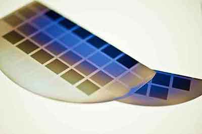
Typical Diced Silicon Wafers
The below image typifies what a diced wafer looks like.
