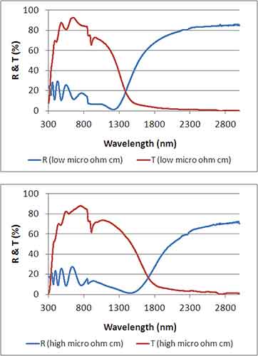
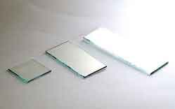
Indium Tin Oxide (ITO) Glass Wafers In Stock

university wafer substrates

Indium-Tin-Oxide (ITO) Coated Substrates For Ellipsometric Research

Typical researchers quote request:

We woulk like to have silicon wafers coated with
indium tin oxide. We would like a thin coating that is tansparent and conductive at the same time. We will use this coated wafer for ellipsometric studies. I was wondering if you can provide us with such coatings?

Reference #100034 for specs and pricing.

Buy ITO Substrates Online and Save!

Indium Tin Oxide Substrates to Study Deformable Mirror for Adaptive Optics Applications

A university scientist requested a quote for the following:

I'm conducting a research that requires the use of some photoconductors, and I would like to ask if it would be possible to have a layer of indium tin oxide (ITO) deposited on one side of the wafer.

I am working on a device used as deformable mirror for adaptive optics applications. I am in the very early phase of my work, and my goal now is to gain experience with assembly and understand the process problems that can arise. For now I am looking for few materials to test, and they are: silicon, gallium arsenide and zinc selenide. The requirements are: high resistivity, thickness not higher than 3 millimeters, round shape, lapped on both sides, and as already mentioned if it was possible to lay a layer of ITO.

Reference #246503 for specs and pricing.

Get your Indium Tin Oxide (ITO) Glass Wafer Quote FAST!

What is Indium Tin Oxide on Glass?

Indium tin oxide (ITO) on glass substrates refers to a thin film coating that combines indium oxide (In2O3) and tin oxide (SnO2) deposited onto a glass surface. It is commonly used in various electronic devices, such as flat-panel displays, touchscreens, and solar cells.

ITO is highly transparent to visible light, making it suitable for applications that require transparency, like displays. Additionally, it has good electrical conductivity, enabling it to function as a transparent conductor. This property is crucial for touch-sensitive screens where electrical signals must pass through the transparent layer to detect touch input.

The deposition process for ITO involves techniques like physical vapor deposition (PVD) or sputtering, where a target consisting of indium and tin is bombarded with ions in a vacuum chamber. This results in the ejection of atoms from the target, which then condense onto the glass substrate, forming a thin, uniform layer of ITO.

ITO-coated glass substrates offer a balance between optical transparency and electrical conductivity, making them ideal for applications where both properties are essential. By applying a voltage to the ITO layer, the conductivity allows for the flow of electrical current while still permitting light transmission.

It's worth noting that while ITO has been widely used, there is ongoing research to explore alternative transparent conductive materials that could potentially replace ITO due to its scarcity and brittleness.

ITO Glass for Resistive Anode Detector

A physics and astronomy Ph.D student asked the following:

Question:

I'm reaching out to you regarding ITO Glass squares I've seen on your site. I would be interested in potentially incorporating these into a resistive anode detector, but would want to know what the porosity of the material is to know if it would be suitable in our vacuum conditions. Would you have any information on this? 

15-20 ohm/sq ITO glass Size: 100mm x 100mm Please specify thickness from 1.1 or 0.7mm
Qty 10

Answer:

ITO layer is deposited via high vacuum sputtering at elevated temperature. Very stable under any vacuum.
No porosity.

Reference #273659 for specs and pricing.

At What Temperature Do ITO Glass Wafers Start Degrading?

A Phd candidate asked for the following quote:

"ITO Glass take a temp of more than 90C?"

Indium tin oxide (ITO) glass can withstand temperatures up to around 200°C, but its electrical and optical properties can degrade above 90°C. The exact temperature limit for ITO glass depends on various factors such as the composition, thickness, and deposition process, among others. It is best to consult the manufacturer's specifications for more information on the temperature tolerance of a specific ITO glass product.

Reference #272563 for specs and pricing.

ITO glass Specifications

Product configuration
Glass / SiO2 buffer (~23 nm) / ITO
ITO coating
Magnetron sputtering
ITO patterning
Photolithography
Size
Any size up to 14”x 16”
Typical sheet resistance

(ohm/sq)
6, 10, 13, 15, 20, 60, 100, 250, etc

(Others are also available for volume production)
Substrate thickness (mm)
0.4, 0.55, 0.7, and 1.1
Pre-patterned
Via photofilm or Cr mask
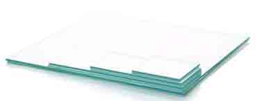
indium tin oxide dimensions

ITO plastic film

Specifications
Product configuration
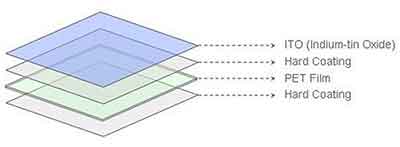
Polyethylene terephthalate (PET) / ITO

PEN / ITO

ITO coating
Magnetron sputtering
ITO patterning
Lithography / Screen-printing / Laser patterning
Size
Sheet / roll (width <=1200 mm)
Typical sheet resistance (ohm/sq)
6, 10, 14, 20, 50, 60, 80, 100,

120, 150, 250, 300, 350, 450, 500
Substrate thickness (mm)
0.125, 0.175, 0.188, 0.21

ITO Physical properties
ITO Work function
4.9 eV (UPS)

We offer consultation for ITO cleaning

4.8-4.9 eV (UPS)

(after exposed to Chloro-based solvents)
ITO thickness
Usually, up to 125 nm
Micro-roughness
RMS 1-2 nm (Digital Instrument 3100 AFM)
Optical transmission
> 85% at 555 nm.

Pilkington FTO glass (TEC series)

We can provide Pilkington TEC15 FTO glass to you. Please find the price as below:

15ohm/sq Pilkington FTO glass (TEC15)
Surface resistance: 12~14 ohm/sq
Thickness of glass: 3.2mm
Transmittance: >82%
Haze: <0.74%
Smoothness: N/A
Size: 50mm x 50mm x 3.2mm

Often used for solar applications.

Nippon Sheet Glass FTO

Specifications
FTO glass manufacturer
Nippon Sheet Glass Co. Ltd., Japan

300mm x 300mm
Typical sheet resistance (ohm/sq) < 7 and 13
Substrate Soda lime float glass
Substrate thickness (mm) 2.2 and 3.1 +/- 0.2
Visible transmission > 77 %
Haze >8 %

Normal FTO glass

Specifications
FTO glass manufacturing PRC
Size
Any size up to 300mm x 300mm
Typical sheet resistance (ohm/sq) <15
Substrate: Clear soda lime float glass
Substrate thickness 2.2 mm

Remark: Customer services including patterning are available. We can offer patterning service for your ITO substrates.

Indium Tin Oxide Material Explained

Indium Tin Oxide Coated Glass for Sale

MAIN PRODUCTS buy online and save!

  • ITO coated glass
  • ITO coated plastic film (PET, PEN, etc)
  • Fluorine-tin-oxide FTO coated glass
  • FPD and ITO glass detergents

indium tin oxide glass with plastic film

ITO Glass Sizes Inlcude But Not Limited To:

  • 300mm x 400mm
  • 400mm x 500mm
  • 450mm x 550mm

indium tin oxide glass sizes

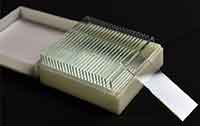
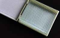
ITO Glass Slides Sizes

  • 25mm x 25mm
  • 25mm x 75mm
  • 50mm x 75mm
We have the following Indium Tin Oxide wafers. Please let us know if any interest you. Or if you know of better pricing elsewhere!

< 10 ohm/sq ITO coated SiO2 wafer
Surface: Polished grade
Size: 4" dia. x 0.55mm

10 $65.90 each
25 $55.90 each
50 $47.90 each
100 $43.00 each

----------
<20 ohm/sq ITO coated SiO2 wafer
ITO thickness: ~ 100nm +/-10nm
Surface: Polished grade
Size: 4" dia. x 1.1mm

25 $34.90 each
50 $30.90 each
100 $25.90 each

----------
<20 ohm/sq ITO coated SiO2 wafer
ITO thickness: ~ 100nm +/-10nm
Surface: Polished grade
Size: 4" dia. x 0.7mm
25 $38.90 each
50 $34.90each
100 $30.90 each

----------
< 10 ohm/sq ITO coated SiO2 wafer
Surface: Polished grade
Size: 4" dia. x 1.1mm
25 $38.90 each
50 $34.90each
100 $30.90 each

----------
< 10 ohm/sq ITO coated SiO2 wafer
Surface: Polished grade
Size: 4" dia. x 0.7mm
25 $43.00 each
50 $38.90each
100 $34.90 each

----------
<7 ohm/sq ITO coated SiO2 wafer
Surface: Polished grade
Size: 4" dia. x 1.1mm
25 $43.00 each
50 $38.90each
100 $34.90 each

----------
<7 ohm/sq ITO coated SiO2 wafer
Surface: Polished grade
Size: 4" dia. x 0.7mm
25 $43.00 each
50 $38.90each
100 $34.90 each

----------
<7 ohm/sq ITO coated SiO2 wafer
Surface: Polished grade
Size: 4" dia. x 0.7mm
25 $51.90 each
50 $43.00 each
100 $38.90 each

ITO Coating Services on Silicon Wafer

A researcher requested the following:

I’d like to know if you provide coating services on silicon wafers? I am interested in coating Indium Tin Oxide (ITO) on one side of a wafer and a thin layer graphite on the other. Is there also alternative coatings for graphite? I am worried that the graphite strip off since it will be exposed to water. The particular wafer I’m interested in is Item 2950 which is undoped, D:100mm, T:50um, Grade: Prime, Float Zone. I would be interested in a quantity of 5 to be coated. Please let me know if that is possible  or if you know who I can contact for the coating. Thank you for taking the time to look at my request. I will reply with more details and specifications if need be.

What I need to do is build a proof of concept which requires  something that “activate” conductivity on different spots on a surface on demand. I have started initially with TFTs in a LCD assembly, but those are both complicated to obtain/manufacture and too much limiting in terms of current. Researching a bit more on TFT, Poly-Silicon/a-Si and everything related to how thin film transistors are made, I got curious about a different approach to my problem which is explained below.

Using the phototransistor concept, I figured I could use a silicon wafer to make conductive zones that I could use to pass current. Imagine a setup where a laser beam hits a small spot at the center of the wafer. Assume that the side on which the laser shines on is charged, say positively (enter the ITO coating, transparent and conductive). The cylindrical Silicon volume above the laser spot would become more conductive due to energy absorption, right? Then touching with a negative probe directly on the other side of the wafer would complete the circuit. If the probe is moved away from the center, this would result in a rapid decrease in current since it is dependent on the resistance. By that logic, there is only a limited spot on the probe side that is “activated”. Moving the laser spot would move the conductive spot per say. Now, there are many aspects I need to understand before committing to this proof of concept. I would really appreciate it if you looked at this setup and tell me if I’m in any way wrong in my understanding. I also have multiple questions regarding that:

  • Is a P or N doped or undoped Silicon make a difference in the amount of current that can go through the wafer?
  • I feel like using PN Junction(s) would only be useful if I want the current to be amplified. Is it necessary if I just need to check the resistance a difference spots? I’d like to test this setup and try to maximize current with only an undoped Si safer.
  • I have read that when Silicon is exposed to air, it would oxidize up to a certain depth and become SiO2 which has a high resistance. Since I am interested in resistance through the thickness only, is this going to be a problem based on the fact that the oxidized layer is extremely small?
  • If I replaced the oxidized layer with something more conductive, what is the point at which the “active” spot becomes too large? It is strongly dependent on layer thickness and resistance. I’m wondering what the best approach is… Does it even need this conductive layer? It’s the reason I am worried about using graphene oxide coating since it would make the whole surface conductive and render it useless.
  • This conductive layer is going to be exposed to air and water and even acid environment. It’s the reason I was interested in graphite. The small SiO2 layer is going to be okay as long as it’s not an HF acid. Do you guys clean the wafers with this prior to applying any coating? 
  • If it works somewhat for laser printers, I think it would also have a chance to work in a flat shape? I’m thinking about the photosensitive drum which is basically a-Si.

I have many more questions and worries but I think this covers pretty well my short term intentions and uncertainties. I will understand if you don’t want to bother reading this long e-mail because this is probably not your problem, so I won’t take offense. Please understand that I’ve been working on this project for more than a year now and that I see a great potential and great applications. I tried contacting friends and professors who are knowledgeable in electrical engineering, and almost all of them simply didn’t have time or didn’t know the answers. Maybe I’m just bad at convincing people…  Either way, I’ll be very grateful and as mentioned before I will definitely pay you back in some way for your help. Maybe even purchase more wafers if necessary or get stock from you that you can’t sell. Hope that this e-mail finds you well. Thank you for reading.

Refernce #228263 for specs and pricing of the following:

ITO coating service
30nm ITO
Sputtering
Size: 100mm dia. x 0.5mm
Graphite coating
We can do reduced graphene oxide coating. 

ITO Glass Substates Used for Electroadhesion

A postdoctoral researcher developing sensors and actuators for robotics requested the followng quote:

I am a researcher scientist working on electroadhesion. I would like to know more about your thin film coating on ITO glass substrates. For my project, I need a thin (~0.5 mm) glass coated with ITO ideally with surface resistivity less than <10 ohm/sq. And I additionally need a thin insulation layer on the ITO, i.e., dielectric layer with a thickness <1um. So my structure will be Glass + ITO + dielectric. The dielectric layer will experience high voltage, therefore I would need high dielectric breakdown for this material. I was wondering if you have a service for dielectric coating on ITO glasses.

Reference #276257 for specs and pricing.

How Do Researchers Use Indium Tin Oxide Substrates?

Indium Tin Oxide (ITO) substrates are used in a wide range of research applications, especially in the fields of optoelectronics and micro/nanoelectronics. Here are some common ways researchers use ITO substrates:

  1. Transparent Conductive Coating: ITO is commonly used as a transparent conductive coating for electronic devices that require a clear or opaque surface. The high transparency and electrical conductivity of ITO make it ideal for applications such as touchscreens, liquid crystal displays (LCDs), and solar cells.

  2. Electrode Material: ITO is a popular choice for use as an electrode material in various electrochemical applications, such as biosensors, fuel cells, and batteries. The high electrical conductivity and stability of ITO make it an attractive option for these types of applications.

  3. Micro/Nano Fabrication: Researchers can use ITO substrates as a base material for micro/nano fabrication techniques such as photolithography, electron beam lithography, and nanolithography. These techniques allow researchers to create complex patterns and structures on ITO substrates that can be used for a wide range of applications.

  4. Optical Applications: ITO substrates are also used in various optical applications such as optical waveguides, optical filters, and micro-optoelectromechanical systems (MOEMS). The high transparency and refractive index of ITO make it a useful material for these types of applications.

Overall, the high electrical conductivity, optical transparency, and other desirable physical properties of ITO make it a versatile material that researchers can use in many different ways, both in fundamental research and in applied technology.

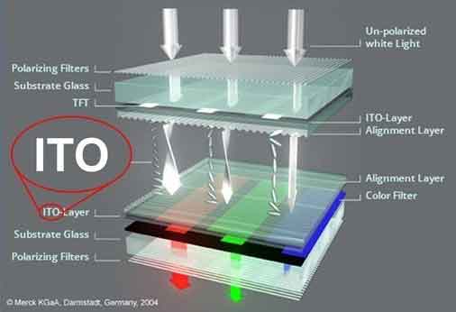
 

What is Indium Tin Oxide (ITO)?

Indium tin oxide is a solid solution of indium(III) oxide and tin(IV) oxidation with unique properties as a transparent semiconductor. The material is available in most volumes, including nanopowder and submicron grades. American Elements produces standard and custom grades of indium tin dioxide. The company also offers MSDS and safety data sheets, as well as a conversion tool.

indium tin oxide device layers

ITO Layers

The melting point of indium tin oxide varies, but it is typically around 2800degF. The composition of the most common indium tin oxide is ca In 4 Sn. ITO is an n-type semiconductor with a large bandgap of approximately four eV, making it a popular material for touchscreen devices. Despite its relatively low melting point, indium tin is highly reactive, making it ideal for a wide range of applications.

Because of its excellent conductivity and transparency, indium tin oxide has become a popular material for the production of thin films. It is also used for glass windows, EMI shielding, and solar cells. Its ratio controls transmittance, which increases with increasing the percentage of indium. When applied to an electronic device, ITO films are particularly useful. These materials are used in electronics. In addition to being an excellent transparent electrode, indium tin oxidide film is effective for solar cells and other devices.

Indium tin oxide is a ternary compound of indium and tin, and is a semiconducting material. Its optical properties make it an ideal choice for high-tech applications such as flat panel displays and IR-mirrors. Its low surface resistance and high film thickness makes it a great material for optical devices. Its conductive qualities make it a popular material for electronic and scientific products.

Indium tin oxide is an excellent transparent conductor and is used in many types of electronic and scientific devices. This tertiary alloy is composed of indium and tin, and is therefore colourless, transparent, and yellow. Its excellent properties make it a highly popular material. It also has excellent electrical and thermal conductivity, and is used in high-performance electronics and in electronics.

What is indium tin oxide? This material is a transparent conducting metal that is both electrically and optically transparent. It is a highly versatile material, which makes it a useful material for electronic devices. It is also a valuable metal in electronics. In addition to being a good conductor, indium tin oxide also has many other uses in the electronics industry. In addition to this, indium tin oxide is a high-quality source of copper, which can help save money on electricity.

Its high transparency is beneficial in many applications, including medical devices. It allows visible light to pass through while reflecting ultraviolet rays. It is used in glass windows, and is also used in aeroplane windshields. In addition to electrical conductivity, indium tin oxide is a versatile material. In addition to conductive electronics, indium tin oxide is used in organic light-emitting diodes and electroluminescent lamps.

Indium tin oxide is an important metal, containing tin, indium, and oxygen. Its high transparency makes it a very desirable material for electronics. Its high optical properties make it an important metal for many other applications. It is a widely used material in liquid crystal displays, touch screens, plasmas, and LCD monitors. Further, it is used as an anti-static coating.

ITO is an alloy of indium, tin, and oxygen. Its electrical conductivity makes it an important material in the optoelectronics industry. It is used to produce displays and other products that use indium tin oxide. It is also used in solar cells and heated defrosting coatings. Its transparent structure makes it an excellent material for LEDs and other electronic equipment.

Indium tin oxide is used in optics and microelectronics. Its optical properties make it an important material for high-performance solar cells. Its name is derived from the Latin word indicum, which means "violet". The material is a popular material in optical systems and semiconductors. The market for indium tin oxide is expected to grow at a rate of 2.8% between the years of 2021 and 2026.

What Indium Tin Oxide (ITO) Specs do I use to Fabricate Electrostatic Actuation System?

A scientist requested the following quote:


I am using these for making flat electrodes for an electrostatic actuation system.

150 mm x 150 mm ITO glass substrates in stock? Thickness <= 0.7 mm, Resistivity <=10 ohm/sq.


Indium tin oxide is a ternary compound composed of indium, tin, and silicon on indium tin oxide glassoxygen. The compound can be classified as either an alloy or a ceramic. The bulk form of ITO is grey to yellow and acts like a metal-like mirror. The properties of this alloy are extremely versatile and can be used in many different applications.

Indium tin oxide (ITO) is a conductive material with a melting point of approximately 2800-3500 degF. It is an n-type semiconductor with a large bandgap of about 4 eV. It is transparent to visible light and highly electrically conductive. It is often used in touch-screen applications.

What Indium Tin Oxide Specs Do I Use? ITO is a mixed oxide of indium and tin. It has a melting point of 2800-3500 degF and is an n-type semiconductor with a wide bandgap of about 4 eV. ITO has excellent electrical conductivity and is transparent to visible light. ITO's optical properties are commonly used in touch-screen applications.

When I need to manufacture electrostatic actuators, I prefer ITO. Its n-type structure makes it easy to fabricate thin films. It is transparent to visible light and is highly electrically conductive. This property makes ITO a perfect material for touch-screens and other applications. Its high conductivity and low conductive properties make it suitable for a wide variety of electronic applications.

The melting point of ITO is 2800-3500 degrees Fahrenheit. Indium tin oxide is a highly transparent material with a high bandgap. ITO is highly conductive and can be used to create electronic circuits. To fabricate electronic actuators, you need to use ITO that is as transparent as possible. You must choose a material that is transparent enough to allow light to pass through.

For electrostatic actuators, you must consider the spec of ITO. The alloy's melting point is 2800-3500 degrees Fahrenheit. It is an n-type semiconductor with a large bandgap of about 4 eV. It is transparent to visible light and electrically conducts, which is why it is commonly used in touch-screens.

ITO is an alloy of indium and tin. Its melting point is 2800-3500 degrees Fahrenheit. It is a n-type semiconductor with a large bandgap of around 4 eV. ITO is transparent to visible light and is highly conductive. Its high electrical conductivity makes it an ideal material for electrostatic actuators.

Indium tin oxide is a highly transparent conducting oxide. Its properties make it an excellent choice for electrostatic actuators. ITO is also a conductive metal. When applied to electrostatic actuators, an electric current can produce a voltage drop in a small space. It is also highly resistant to moisture, so you don't need to worry about corroding the electrodes.

The electrostatic actuator involved in the present invention comprises an electrode and an oscillating plate. The electrode is placed across a gap and applied a voltage to the oscillating plate. The electrode and the plate are electrically connected via a dielectric film, which is formed when indium tin oxide is deposited. When the electrode is positioned across the gap, an electric field is generated between the electrode and the oscillating plate.

When fabricating electrostatic actuators, the sensitivity of the membranes is very important. This sensitivity allows the device to detect changes in the membranes without the need for any external power source. It can also be fabricated with indium tin oxide and other materials. These devices can be manufactured using high-performance and high-precision components.

What Indium Tin Oxide (ITO) Wafers to use for High-Power Lasers and electro-optics for 3D Printing?

A university scientists requested the following: What ITO wafers using high-power lasers and custom electro-optics in 3D printing. In this capacity, we are very interested in your large stock of optical materials. Right now however, we are interested in something that does not appear to be off the shelf for you. Your ITO on glass is an excellent test substrate for us due to its low cost. However, the ideal size for us would be 40x40x2mm. If the thickness is a challenge, we could accommodate 40x40x1mm.


The following ITO wafers will work:

20 ohm/sq ITO coated glass
Japan display grade
Surface: Polished grade
Size: 40mm x 40mm x 1.1mm0

Please ask us for pricing.

ITO is Compatible With Both Electro-Optics and High-Power Lasers

The first question that arises in our mind is, "What are Indium Tin Oxide Wafers?" The answer is that these materials are highly porous and have a high melting point. The main benefit of these materials is that they are compatible with both electro-optics and high-power lasers. These metals are also known as amorphous silicon.

indium tin oxide compatability with electro-optics and high-power lasers

Indium tin oxide wafers are made from a highly porous material. Its refractive index is tuned using a carrier-dependent Drude model. The amount of indium atoms in ITO is higher than in Silicon. This gives it a wider bandgap. However, the material has a low mobility of electrons and a low refractive index.

This material can be used to tune plasmonic absorbers and switch plasmons. Its ability to amplify light enables it to be a versatile photonic component. In addition to being a versatile metamaterial, ITO is also a highly conductive material. Its properties make it ideal for touch-screen applications. Airbus cockpit windows are coated with ITO to prevent thin-film interference.

Another advantage of ITO is that they are tunable, which means that the tunable cavity will allow for future modulators and optical sources to have higher mobility. These qualities make Indium Tin Oxide Wafers excellent materials for High-Power Lasers and electro-opstics. While this is a basic explanation of how ITO is used, the answer is more complicated.

Indium Tin Oxide Wafers are used in a number of applications. Indium Tin Oxide (ITO) is used for high-power lasers and electro-optics. Its unique properties make it a great material for both high-power lasers and electro-optical devices. Its use in these applications is expanding rapidly, and there are many exciting possibilities.

Indium Tin Oxide is a mixed oxide with a melting point of 1526-1926 degC. It is a n-type semiconductor with a large bandgap. Its transparent nature makes it ideal for touch-screen applications. Its low electrical resistivity makes it suitable for electro-optics. Its transparent properties make it an excellent material for these devices.

The material has a limited supply and is very expensive. It is also difficult to fabricate ITO wafers in large quantities, but the new materials are now available. Some of the most common ITO products are used in lasers and electro-optics. In addition to tin, ITO is another common material. Its insulating properties allow it to resist heat and to be highly transparent in certain conditions.

The Indium Tin Oxide wafers used in electro-optics and High-Power Lasers are a mixed oxide with a high melting point. Its high transparency allows it to operate as a semiconductor with larger optical bandgaps. Indium Tin is a n-type semiconductor with an extremely large bandgap. It is transparent to light and low in electrical resistance. In addition, it has excellent thermal conductivity.

The Indium Tin Oxide Wafers are used to create high-power lasers. They are also used to tune plasmonic absorbers. This material is also used in high-performance electro-optic modulation. This material is commonly seen in a variety of different applications. Its melting point is approximately 1.5 oC. Its thickness is approximately 0.4 ocm.

Indium Tin Oxide is a transparent conductive oxide that is extremely transparent to light. Its high transparency allows it to be used in a variety of applications. Its applications include touchscreen displays, liquid-crystal displays, and solar cells. They can also be used in defrosting aircraft windshields. The heat produced by the film produces the radiation required to illuminate the aircraft.

Indium Tin Oxide is an extremely rare element. It is used to manufacture semiconductors and high-power lasers. It is also a valuable component in a wide range of other applications. Its properties make it an ideal material for use in photonics. Its thin film makes it easy to manufacture and has a low resistance to electric fields.

Indium Tin Oxide Market Trends

Indium Tin Oxide Market Trends are expected to expand at a moderate-to-high pace during the forecast period. Companies are focusing on the development of innovative products and are modestly reducing their R&D budgets. The companies are also carefully launching their marketing strategies and strengthening long-term contracts. Further, the companies are increasing M&A activities to strengthen their position in the market. Moreover, the companies are focusing on the development of sustainable supply chains and bolstering their manufacturing capacities.

The consumer electronics industry is one of the key drivers of the global indium tin oxide market. These devices include smart cars, touch panels, and attractive displays. In addition, favorable government policies and extensive R&D activities have helped reduce the cost of ITO production. Hence, the report will help vendors in devising an efficient business plan. This report is also essential for any company who is interested in entering the indium tin oxide market.

Consumer electronics are another important driver of the global indium tin oxide market. This product is used in touch panels, displays, and other electronic products. The consumer electronics industry is expected to grow at a moderate rate during the forecast period. Indium tin oxide market in APAC is expected to grow at a CAGR of approximately 6.1% during the forecast period. Besides presenting regional opportunities, the indium tin oxide market report covers the competitive intelligence, marketing gaps, and regional growth opportunities.

A comprehensive analysis of the global indium tin oxide market provides key insights, strategic analysis, and market forecasts. Indium tin oxide is an alloy of indium, tin, and oxygen, with a higher share in industrial applications than in consumer markets. It is an ideal material for a range of electrical applications and is used in the production of semiconductors, LCD screens, and other consumer electronics.

The global indium tin oxide market report includes a high-quality research of the industry. It offers detailed information on the current and future market dynamics. The report covers the major players and their products, including the cost-effective methods and materials. The research includes the company-level analysis of the industry. Further, the market study reveals the key players in each region. The report highlights the growth strategies of the vendors.

The Indium tin oxide market is expected to grow rapidly in Asia-Pacific. The region is expected to grow at a steady rate for the next few years. The South Korean country is one of the leading manufacturers of electrical components, and it generated USD 21,838 million revenue from displays alone in 2019. Moreover, the government's support for the industries will also increase the demand for indium tin oxide in the region.

The report analyzes the global indium tin oxide market. It highlights the various types, applications, and regions. It provides an in-depth study of the indium tin oxide market and its future prospects. It also highlights the main companies in the industry. Some of the other segments of the indium tin oxide market are electrochromic displays, heat reflective coatings, and energy-efficient windows.

The report includes market data by region and by country. Its comprehensive coverage of post-pandemic forces, graphical representation, and revenue are included in the report. The regional market forecast is based on the latest data, and the analysis is accompanied by a discussion of the factors driving the growth. The regional segmentation is based on demand, supply, and geography. It also shows which regions are the fastest-growing.

The report includes a detailed analysis of the global Indium tin oxide market and its competitive landscape. Its market analysis discusses the current and future trends of the indium tin oxide industry. It also provides a comprehensive and insightful study of the indium tin oxide market and its competitors. The report also analyzes the key trends and the opportunities that the market is experiencing. The global Indium tin oxide market has tremendous potential.

The Indium tin oxide market is anticipated to grow at a CAGR of x. It will account for $x billion in 2020. The report offers detailed information on the major players in the market. It also identifies the most promising geographical segments for the indium tin oxide industry. It also highlights the key drivers affecting the indium tin oxide market and the opportunities it presents for the industry.

Indium Tin Oxide Coated PET Sheet

ITO-coated PET sheets are available in different shapes and sizes and have a surface resistivity of between 60 and 300?/sq. These sheets are available in several standard grades and meet the relevant ASTM standards. They can also be custom-packaged for customers who require more than standard sizes. They also provide safety and technical information such as MSDSs and a conversion tool. In addition, these materials are recyclable.

indium tin oxide with pet layers

ITO-PET is an optically transparent and electrically conductive film that is covered with a thin, transparent film that can be peeled off. This material can be used to fabricate flexible OLEDs and as a reference anode for conventional flexible polymer-based OSCs. Its transparent film can also be used to manufacture a number of different types of solar cells.

Indium Tin Oxide-coated PET sheet is a transparent conductive film or liquid, and it is made by coating PET with Tin Oxide. The resulting coating is a conductive patterned layer that is widely used in the converting industry. This transparent, conductive film is also easy to cut with a laser cutter or scraper. Indium-Tin Oxide-coated PET is the ideal choice for applications where the material is exposed to heat.

This product is a thin layer of Indium Tin Oxide on a PET sheet, which is both transparent and electrically conductive. The film is protected by a thin transparent film that can be peeled off. It is also a reference anode for conventional flexible polymer-based OSCs. Indium Tin Oxide-coated PET sheet is available as a roll-to-roll or a single sheet product.

Indium Tin Oxide-coated PET sheet is manufactured by applying a thin layer of Tin Oxide on PET. This conductive material is used in a variety of applications such as solar cells, LEDs, and LCDs. It can also be cut with a laser or scraped off with a flat blade. These films are commonly used in the converting industry for a number of different reasons.

Indium Tin Oxide-coated PET sheet is a high-quality, conductive polymer that is made from a transparent conductive polymer. This material is a popular choice for a wide range of products. Its low resistance makes it suitable for applications requiring electrical conductivity. Its low resistance allows it to be cut to a very thin sheet using a laser. Indium Tin Oxide-coated PET Sheets are flexible and resistant to temperatures up to 120 oC.

Indium-Tin Oxide-coated PET sheet is a common choice for solar-panel production. These transparent sheets are a great choice for many applications, including solar panels, LCDs, and LEDs. The transparent coating protects the Indium Tin Oxide, which is a clear, conductive material. The film can be easily peeled off with a flat blade or cut with a laser.

ITO-coated PET sheet is a conductive material that is both transparent and electrically conductive. It is a good choice for a variety of applications involving electronics. Indium Tin Oxide-coated PET sheet is highly flexible and can be cut using a laser. It can be easily laminated with PE to make it stronger. The thickness of the film varies between different manufacturers.

The Indium-Tin Oxide-coated PET sheet is a transparent conductive film or liquid. It is optically transparent and electrically conductive. It can be peeled by using a laser or a flat blade. It is also used in the manufacturing of LCD/OLEDs. The film has a thin, transparent layer on it which protects the Indium Tin Oxide coating.

ITO-coated PET sheets are commonly used for a variety of applications. They are highly transparent and have high electrical conductivity. They are also widely used in microelectronics. Its versatility has made them a popular choice for touch-screen applications. There are also a number of products made from this material. They are often used in optical fibers, displays, and in lasers.

Indium Tin Oxide (ITO) Coated PET Sheet

Coating Properties:

  • Specified ITO Sheet resistivity – ≤ 15 ohms/sq
  • Typical ITO Sheet resistivity – 8 10 ohms/sq
  • Transmittance at 550nm – ≥ 75%
  • ITO film Thickness – 1400-1500 Å
  • Sheet Thickness – 0.175 mm or 175 micron
  • Haze – NA
  • Heat resistance (R/R0) - ≤1.3 (@130°C, 30min)
  • Hear storage (R/R0) - ≤1.3 (@90°C x 250hrs)
  • High humidity storage (R/R0) - ≤1.3 (@60°C x 250hrs, 95% RH)
  • Heat cycle (R/R0) - ≤1.3 (@-30°C 85°C x 50 cycle)
  • Adhesive- Excellent (@1.0kg x 25 cycle with cloth)
  • Surface check - Smooth, no holes, no patches and no stain
  • Storage temperature - -30°C +40°C
  • Brand – UniversityWafer, Inc.

Physical Properties:

  • Configuration – Polyethylene terephthalate (PET) / ITO
  • Substrate – Optical clear grade PET film / Hardcoated PET film
  • Surface finished of glass – N/A
  • Passivation layer – No
  • ITO coating method – Magnetron sputtering at elevated temperature under vacuum
  • ITO work function – 4.8 4.9eV (measured by UPS) after proper cleaning
  • Surface Roughness – RMS1 10 nm, depend on the various product
  • Packing - Sheet/roll form

Indium Tin Oxide (ITO) Coated PET Sheet Product Series: TIPZ

Coating Properties:

  • Specified ITO Sheet resistivity – 60 ohms/sq
  • Typical ITO Sheet resistivity – 70 ohms/sq
  • Transmittance @ 550nm – ≥ 8 %
  • ITO film Thickness 350 to 370 Å
  • Sheet Thickness – 0.175 mm or 175 micron
  • Haze – NA
  • Heat resistance (R/R0) - ≤1.3 (@13 °C, 30min)
  • Hear storage (R/R0) - ≤1.3 (@9 °C x 250hrs)
  • High humidity storage (R/R0) - ≤1.3 (@6 °C x 250hrs, 95% RH)
  • Heat cycle (R/R0) - ≤1.3 (@-30°C 85°C x 50 cycle)
  • Adhesives - Excellent (@1.0kg x 25 cycle with cloth)
  • Surface check - Smooth, no holes, no patches and no stain
  • Storage temperature - -30°C +40°C
  • Brand – UniversityWafer, Inc.

Physical Properties:

  • Configuration – Polyethylene terephthalate (PET) / ITO
  • Substrate – Optical clear grade PET film / Hardcoated PET film
  • Surface finished of glass – N/A
  • Passivation layer – No
  • ITO coating method – Magnetron sputtering at elevated temperature under vacuum
  • ITO work function – 4.8 4.9eV (measured by UPS) after proper cleaning
  • Surface Roughness – RMS1 10 nm, depending on the various product
  • Packing - Sheet/roll form

Is Indium Tin Oxide (ITO) Conductive?

ITO is composed of the elements indium, tin, and oxygen and is a ternary compound. The material is transparent, colourless, and yellowish in appearance, and is extremely conductive. It can be processed using various process technologies. Here are some of the methods used to make ITO. Read on to find out more. Its properties include: A low melting point, high conductivity, and low cost.

indium tin oxide conduction

The most common form of indium is indium tin oxide, which is 90 percent indium and ten percent tin oxide. Its combination of conductive properties and transparency makes it an ideal material for electronic applications, including mobile phones, LCD monitors, and other electronics. This substance is also used in various types of photovoltaic cells and solar cells. This enables ITO to be used in various applications such as LCD displays, LEDs, and fluorescent lights.

ITO is a n-type semiconductor, with a large bandgap of around 4 eV. This material is transparent to visible light, and has high electrical conductivity. This material is used in touch-screen displays and other electronics. It is transparent to ultraviolet light, making it ideal for

Is Indium Used in Iphone?

Apple uses indium as a coating for its touch screen. Other cell phone manufacturers also use indium?

The iPhone is a touchscreen phone, so it doesn't need a stylus. Instead, it detects the touch by detecting the presence of your finger. The touchscreen is made up of glass coated in indium tin oxide, or ITO. The ITO is the most commonly used material in LCD screens, touch screens, flat screen TVs, and solar panels. However, it is not completely suited for such devices, so research.

How much indium is left in the world?

This material is rare and the U.S. government projects that indium mines will run dry by 2020. It is a good alternative, but many are worried that its use will reduce the quality of iPhones. Here's what you need to know about the precious metal. Read on to learn more. Is indium used in iPhones?

Indium is a rare mineral and is mostly used for the electrodes in electronic devices. This metal is not widely available, so it is used in high-tech devices. This metal has a high melting point and is often referred to as indium oxide. The indium tin oxide used in touchscreens is optically transparent and electrically conductive. This is a natural material that can be found in abundance.


ITO high-light transmission and high-conductivity are great for Liquid Crystal Displays (LCD). ITO films exhibit excellent transmittance and high-conductivity characteristics. These properties make ITO the best choice for transparent electrodes in Liquid Crystal displays.

However, ITO isn't without its problems. Alternative solutions are currently being developed and finding success in the market, which is lowering the cost of ITO and increasing its adoption. As a result, Nanomarkets predicts that sales will continue to increase in the next few years before declining.

indium tin oxide glass cleaning

Bare (unpatterned) indium-tin-oxide (ITO) glass
(e.g. 15 ohm/sq.; 25 mm x 25 mm

Patterned indium-tin-oxide (ITO) glass
(e.g. 15 ohm/sq.; 25 mm x 25 mm

Bare ITO coated plastic film [PET, PEN]
Patterned ITO coated plastic films [PET, PEN]
Discount 60 ohm/sq ITO coated PET film (0.125mm)

How Do You Dice Indium Tin Oxide Substrates?

A scientist requested the following:

Question:

purchased some ITO coated glass wafers and have been having problems when I try to dice my parts. I bond the glass wafers to a silicon wafer using an adhesive (SU8). To do this I use an elevated temperature (110C) and pressure ~2000-2500N. Next, I dice the wafers using a dicing saw. I have performed this process without issue with borofloat glass, however, with these wafers whenever I dice my parts the glass cracks.

Can you please provide more information about the type of glass used? I believe the part number is 34490. They are <10 ohms/square SiO2 wafers. Can you provide any guidance about the strength of the glass and possibly different parameters to adjust to prevent the glass from cracking?

Aternatively, can you coat borofloat wafers or provide me with ITO coated glass wafers that will withstand my process?

Answer:

The glass substrates are made by LCD display grade float glass, different from Borofloat. To cut the ITO glass, it is not required to cut through the substrates. A light scratch on the glass surface is good enough. The glass can be then spitted easily by hands.
Currently, we are planning borofloat or BK7 for ITO coating but not yet ready.

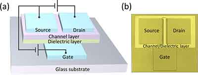
Could We Use Indium Tin Oxide Instead of Silicon For Making Transistors?

Aside from its obvious benefits, Indium Tin Oxide has many other benefits as well, including its high electrical conductivity and similar electron configurations to silicon. It is transparent, and electrons move easier in an amorphous state. This is why Intel is looking into this material as a possible replacement for silicon in transistors. If it works, it could make the technology much more affordable than using other materials.

glass substrate source drain and gate transistor

Indium Tin Oxide is a transparent conducting metal, which makes it a great alternative to silicon for making transistors. The material can be easily deposited as a thin film. When it comes to choosing a transparent conducting material, it's important to find the right compromise between transparency and conductivity. As the thickness increases, the charge carriers in the material are trapped inside, reducing the transparency. ITO thin films are most commonly deposited by physical vapor deposition (PVD) and sputter deposition techniques.

However, the potential for a new semiconductor technology is still unclear. There are several potential alternatives to silicon for making transistors. Indium-Tin Oxide is an excellent alternative because it is highly transparent, environmentally friendly, and cost-effective. It has the same high mobility as silicon, but it can be more expensive and more complex. If the properties of the indium-Tin Oxide compound are perfected, we should see it on the market within a few years.

Its higher mobility enables it to be fabricated at room temperature. Another viable alternative is indium-doped zinc oxide. Both are inexpensive, and have similar properties. Aluminum-doped zinc oxide can be used in a few applications. Finally, conducting polymers are being developed to replace the crystalline silicon. They are cheaper, more flexible, and environmentally friendly.

Indium Tin Oxide is an alternative material that is both transparent and electrically-conductive. This material is easily deposited, making it an ideal candidate for thin-film transistors. The disadvantage of ITO is its low thermal conductivity. Indium-doped zinc oxide has similar properties. A combination of these two materials can be used to build a thin film in the same thickness as silicon.

The material is a transparent conducting oxide with high transparency. This means it is easier to deposit a thin film. Its comparatively high mobility is advantageous in transistors. But it is not clear whether it can replace silicon as the best semiconductor for this application. It is not known if the material can replace silicon for making transistors. Some researchers have tried using it in some other applications.

As a semiconductor, ITO is a transparent, electrically-conductive, and optically-transparent material. The advantages of ITO over silicon are a combination of high thermal conductivity and low mobility. The advantages of ITO over silicon are that it is cheaper, environmentally-friendly, and flexible. It can also be deposited as a thin film. The key is that it's transparent and does not change color.

Indium Tin Oxide is a ternary material consisting of indium, tin, and oxygen. It is an alloy with two main elements: indium and tin. Its oxidation state gives it a high concentration of charge carriers. While the indium tin oxide inherently has high mobility, it is less efficient as a semiconductor.

Although it is difficult to find ITO that meets the required electrical and optical requirements, the material is a promising alternative to silicon. In addition to the high-density version of silicon, ITO is also more flexible and eco-friendly than silicon. As a result, it is a great substitute for both silicon and indium. But it must be noted that ITO does not have the same properties as a semiconductor.

IGZO has several advantages over silicon. The material is amorphous and is more resistant to bending. This means that it is more flexible than silicon, and it is more affordable for consumers. Amorphous materials are more efficient than silicon in semiconductors. They are also cheaper than the silicon-based ones. In addition to their other advantages, IZTO is also transparent and can be used in liquid crystal displays and organic light emitting diodes.

Why FTO substrate is more frequently used than ITO?

FTO, or fluorine-doped tin oxide, is a transparent conducting oxide (TCO) material that is frequently used as a substrate in thin film solar cells and other optoelectronic devices. There are a few reasons why FTO is more commonly used than ITO, or indium tin oxide, which is another commonly used TCO material.

One reason is that FTO has a lower resistivity compared to ITO, which makes it more conductive. This is important in optoelectronic devices because it allows for better charge transport and higher device efficiency.

Another reason is that FTO is more chemically stable than ITO. It is less susceptible to degradation when exposed to oxygen and moisture, which makes it more durable in practical applications.

Finally, FTO is generally less expensive to produce than ITO. This is because the raw materials used to make FTO are more abundant and less expensive than the raw materials used to make ITO.

Overall, FTO is a more practical and cost-effective choice for many optoelectronic applications compared to ITO.