What is Gallium Nitride on Sapphire?
Silicon has long been the substrate of choice for power electronics, but due to advancements in research, GaN has superseded silicon. The reason for this change is that GaN is considered a wide-bandgap material. This means that it has a high breakdown voltage and excellent efficiency when performing at high temperatures.
Why Use GaN Wafers?
Gallium Nitride on sapphire is the ideal material for radio energy amplification. It offers a number of benefits over silicon, including a higher breakdown voltage and better performance at high temperatures.
If you need a UniversityWafer, Inc. product that will provide you with high quality and reliable results we suggest using our Gallium Nitride substrates.
Get your GaN on Sapphire Quote FAST!
Gallium Nitride (GaN) Epitaxial Grown on Al2O3 Substrates
GaN is a binary III/V direct bandgap semiconductor commonly used in bright light-emitting diodes since the 1990s. The compound is a very hard material that has a Wurtzite crystal structure. Its wide band gap of 3.4 eV affords it special properties for applications in:
- optoelectronic
- high-power devices
- high-frequency devices
For example, GaN is the substrate which makes violet (405 nm) laser diodes possible, without use of nonlinear optical frequency-doubling. Its sensitivity to ionizing radiation is low (like other group III nitrides), making it a suitable material for solar cell arrays for satellites. Military and space applications could also benefit as devices have shown stability in radiation environments.
Gallium Nitride transistors can operate at much hotter temperatures and work at much higher voltages than gallium arsenide (GaAs) transistors, they make ideal power amplifiers at microwave frequencies.
Recently a reseachers asked about the following GaN spec:
Researcher
I am interested primarily in this:
2" bulk GaN wafer, Thickness is 350um .N-type(un-doped),A level
Can you give me more details on the technical synthesis of the material, dislocations rate, the value of the residual doping, the surface polarity, the number of macro-defects?
Response
We have:
2" bulk GaN wafer, Thickness is 350um .N-type(un-doped),A level
4" GaN template, Thickness is 4um,N-type(un-doped)
Non-Polar Freestanding GaNSubstrates (A-plane), Thickness is 350um,5mmx10mm
HEMT Structure on Sapphire, 2 inch
2" AlN wafer on Sapphire
2" GaN wafer on Sapphire(Undoped),thickness is 4um
2" GaN wafer on sapphire (Si-doped), thickness is 4um
2" GaN wafer on sapphire (Mg-doped), thickness is 4um
HEMT stucture on Si substrate,2inch
HEMT stucture on SiC substrate, 2inch
2 " Gallium Nitride Blue orGreen LED wafer
The specifications ,please see the attached .
Gallium Nitride Lite Emitting Diodes

No Heatsink? No Problem!
New IC are on the market. The gallium nitride (GaN) devices support display and appliance power supply applications that don't require a heatsink for continuous power of up to 75 Watts
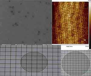
Wafers for GaN Nanophotonics
Scientists were looking to build a research program around Gallium Nitride nanophotonics. They were interested in GaN on sapphire with a thickness of 100 and 150nm.
UniversityWafer, Inc. Quoted:
GaN nanophotonics,the materials for nano photonics, 4'' Un-doped Gallium Nitride on SSP
sapphire with a thickness of 100 and 150nm,Qty. 15pcs
What Gallium Nitride (GaN) Wafer Should I use to Fabricate High-Electron-Mobility-Transistors
A researcher contacted us for the following: We are looking for the following layer stack: UID GAN (4,000-5,000 nm 4 - 5 micron) AlGaN Transition Layer AlN Nucleation Layer Si Substrate (111) can you let us know whether its available and with which wafer sizes ? Polished GaN surface is required.
UniversityWafer, Inc.
Yes,It available and can supply,We do this type of HEMT GaN Epi stack on 4'',6'' and 8'' Silicon <111> wafer.
Epi surface roughness </=0.5nm,Pls confirm you still need the epitaxial finished surface to be polishing?
Researcher:
Thanks very much for your fast reply. You are completely right, the epitaxial finished surface would not need to be polished, my mistake.
Also, you spotted correctly that we only need the unintentionally doped GaN at the top of the layer stack and no further layers for high-electron-mobility-transistors.
May I ask you to clear these issues for me:
- Do you offer 4 or 5 micron UID GaN?
- Do you have information on the surface roughness of the UID GaN?
- The thickness of the AlN and AlGaN transition layer will be 150 nm and 1500 nm, respectively?
- For what prize can you offer one or two 2" wafer?
- We will need to do some prototyping and would then order more.
- Do you offer 4 or 5 micron UID GaN : -- We offer 4um GaN
- Do you have information on the surface roughness of the UID GaN : -- Roughness less than 0.5nm
- The thickness of the AlN and AlGaN transition layer will be 150 nm and 1500 nm, respectively ? : -- Yes
- For what prize can you offer one or two 2" wafer ? : -- 6'' wafer can be supply at qty. 2
UniversityWafer, Inc.
Please contact us for pricing.
What is Refractive Index of GaN?
he refractive index of gan is an important property to study when using a goniometer. This property varies with the energy of electrons and photons. Figure below shows the corresponding reflection spectra. The fitting parameters were eV and e. Optimal indices were obtained after analyzing both reflection spectra. They show the relationship between the two properties.
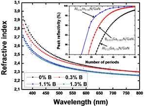
For a material that has a pleochroic refractory index, it must be a dielectric. For example, an opaque glass will absorb a light beam. Moreover, a transparent object will reflect a light beam. The light that passes through a thin glass or a dense liquid is shifted from one axis to another. This phenomenon is known as polarization.
The refracting power of a semiconductor is directly proportional to its refractive index. This is due to its excellent thermal conductivity and low compressive and tensile stress. Its refracting power is proportional to its crystal thickness and shape. The refracting index of alumina is 1.3. The compound is used in solar cells and spacecraft. The refracting properties make it a viable material for many applications.
Besides the Burstein-Moss effect, plasmonic effect, and electron concentration also affect the refractive index of a germanium-doped layer. This method assumes a rigid translation between the real and imaginary parts, while the bending and rotational movements of a thin plate are uniaxial. This method is theoretically rigorous, but should still work for energies below the bandgap.
Measurement Data for Gallium Nitride Available
If you want to receive Measurement data, the measurement charge is as follows:
- DCXRD Rocking curve
- Room Temperature Raman Spectra
- PL mapping (Accent Model)
- AFM ( 5x5 um, 20x20 um )
Reference #115733 for more info and pricing.
Gallium Nitride on Sapphire (GaN)
Gallim Nitride (GaN) radio frequency power is five times more powerful than last generations material including silicon. New GaN technological gains should result in much lighter, smaller and powerful electronic devices.
Below are just some of the GaN on Sapphire specs that we have. Please email us the specs and quantity that you need quoted.
GaN epitaxial wafers consist of GaN layer on 6H-SiC substrate. 50 mm diam on axis, n-type, GaN thickness ~0.5 um
GaN layer on sapphire, 50mm diameter on-axis, n-type, GaN thickness 0.5-10 um.
GaN/AIN/SiC epitaxial wafer consisting of GaN layer on AIN layer on 6H silicon carbide.
50mm in diameter on-axis, n-type.
GaN thickness ~(0.5-0.8) um.
AIN thickness ~0.1um.
GaN/AIN/AI2O3 epitaxial wafer consists of GaN layer on AIN layer on sapphire.
50mm in diameter, on-axis, n-type, GaN thickness ~(0.5-0.8) um, AIN thickness ~0.1 um.
Buy Online!
| Item |
Dia |
Typ/Dop |
Ori |
GaN (μm) |
Al203 (μm) |
Al2O3 Plane |
Pol |
Other Specs |
| 2859 |
100mm |
N/Si |
<0001) |
5.0 |
650 |
c |
DSP |
|
| 2521 |
50.8mm |
N/Si |
<0001> |
5.0 |
430 |
c |
DSP |
|
| 2857 |
50.8mm |
P/Mg |
<0001> |
4-5 |
430 |
c |
DSP |
Useable surface area: > 90%, TTV: = 10um, BOW: = 10um, Warp: = 10um |
| 2856 |
50.8mm |
P/Mg |
<0001> |
4-5 |
430 |
c |
SSP |
|
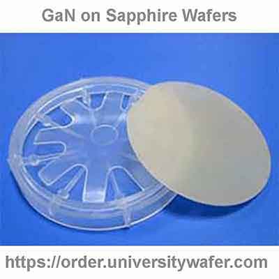
Above is a Single Side Polished GaN Wafer with single wafer carrier.
Ask us about strained heteroepitaxial growth and epitaxial overgrowth!
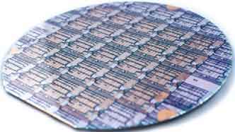
Gallium Nitride, otherwise known by its chemical symbols as GaN, is a the ideal substance for radio energy amplification, which can work to enhance devices like radars and jammers. In past years, silicon was the substrate of choice for power electronics, but due to advancements in research, GaN has superseded silicon. The reason for this change is that GaN is considered a wide-bandgap material. This means that it has a high breakdown voltage and excellent efficiency when performing at high temperatures. If you need a UniversityWafer product that will provide you with high quality and reliable results we suggest using our Gallium Nitride substrates.

A thin layer of GaN is used on LED lights to pass an electric current which causes the bulb to light

GaN’s high power density is used to produce sound quality in class-D sound amplifiers

GaN boosts amplification of microwave signals in radar with higher voltage than silicon
What is Gallium Nitride Used For?
Gallium nitride is a semiconductor with a wide bandgap. It is also known as GaN. Its properties make it an ideal material for power transistors and integrated circuits. These semiconductors are low-cost and allow for higher switching frequencies. This allows for smaller power supply components such as the main transformer, EMI filter components, and bulk capacitors.
Gallium nitride is a semiconductor material with high melting points. It has great potential as a base 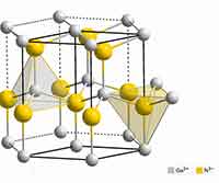 material for semiconductors in high-temperature settings. It also accepts magnesium, making it a p-type semiconductor. It can be synthesized from pure gallium and ammonia. The combination of these two materials, heat, and pressure, results in a solid material.
Gallium nitride is a direct-bandgap semiconductor that is fast and efficient. It is also resistant to high voltages, so it is ideal for power-related applications. It has a wider bandgap than silicon, which means that it can operate at higher temperatures than silicon MOSFETs. It is used in optical devices as well, and its future applications will be sensor technology.
As a semiconductor material, gallium nitride has potential to replace silicon as the heart of electronic chips. This material is non-toxic and compatible with human cells, making it ideal for biomedical implants. With this added benefit, the technology will become more versatile and cheaper. You might be wondering: What is gallium nitride, anyway? So, what are it used for?
Its unique characteristics make it the ideal semiconductor material for a wide variety of applications. Its high-frequency and low-voltage capabilities make it an ideal choice for LEDs and other high-frequency products. Using this material in these applications can greatly increase the efficiency of electronic systems. Its high-frequency and ultra-low resistance and capacitance properties makes it a great choice for optoelectronics.
The technology behind gallium nitride is a promising semiconductor material. The combination of gallium and nitrogen is an ideal semiconductor material. GaN is the ideal material for power electronics. Its high-temperature resistance makes it a great material for high-frequency applications. Further, it is also useful for sensors. It is a component of LEDs and is a key component of mobile devices.
What is gallium nitride? usturoi para: What is gallium nitide used for?para: The material is a key component of various electronic devices. Its properties make it an ideal choice for power electronics and sensors. Moreover, it has been shown to increase the efficiency of semiconductors. Aside from this, the technology can be useful in many more fields.
Galvanized gallium is a high-temperature-resistant, high-temperature semiconductor. The best applications for gallium nitride are conductive, electrical, and optical. While the material is conductive, it does not conduct electricity. It is used to create the blue light needed for Blu-ray disc reading. However, this material is useful in some other applications. Aside from advancing 5G technologies, gallium nitride is being widely adopted.
As a high-temperature semiconductor, gallium nitride is an excellent candidate for various applications. Its melting point and high-temperature operating characteristics make it an excellent choice for power amplifiers in microwave and THz bands. Among its other uses, it has been used in LED lighting and in the production of Blu-ray disc readers. In the near future, it will also be used in sensors and as a source of energy.
For semiconductors, gallium nitride is a good candidate for 5G. It is suitable for mmWave and sub-6GHz frequencies. It is also used in antenna arrays, which requires high power and high heat dissipation. Ultimately, this material is a better choice than silicon in the market for 5G and other wireless technology applications. Aside from these, it is a better candidate for radio frequency (RF) communications and for the fabrication of RF transceivers.
A semiconductor with a wide bandgap is called gallium nitride. It is a good material for transistors and other semiconductor devices. Its high cutoff frequency and high thermal conductivity make it an excellent semiconductor material. Further, it is highly resistant to radiation, and can be used for many applications. So, what is gallium nitride used in?
Gallium Nitride, otherwise known by its chemical symbols as GaN, is a the ideal substance for radio energy amplification, which can work to enhance devices like radars and jammers. In past years, silicon was the substrate of choice for power electronics, but due to advancements in research, GaN has superseded silicon. The reason for this change is that GaN is considered a wide-bandgap material. This means that it has a high breakdown voltage and excellent efficiency when performing at high temperatures.
Gallium Nitride Specs Used for RF Schottky Barrier Diode (SBD) Application
A researcher asked us to quote a GaN substrate for their RF SBD application. UniversityWafer, Inc. quoted the following spec:
Gallium Nitride on Silicon Wafer for RF SBD application
100mm GaN on Si for GaN RF SBD / 10ea
Price $Depends on Qty
Reference #262996 for pricing.
What are the FWHM of XRD line concentration of Mg and conductivity of GaN layers?
Please see below data for your reference:
FWHM of RC for the symmetric (002) reflection:~ 250 arcsec
FWHM of RC for the symmetric (102) reflection:~ 300 arcsec
Concentration of Mg : > 6x1016 cm-3
Conductivity : ~10Ω·cm
Please contact us for pricing reference #257591
2" GaN/Al2O3, Undoped,4-5 µm GaN on 2" (0001) SSP
2" GaN/Al2O3, Mg-doped,4-5 µm GaN on 2" (0001) SSP
Gallium Nitride (GaN) based Electronics
Fabricating electronic devices from Gallium Nitride instead of silicon, power consumption can be significantly reduced by emitting light into the ultraviolet range, which has shorter wavelengths. Researchers have succeeded in developing semiconductor compound semiconductor technology by using copper iodide semiconductors (CuI) made of copper, Cu and iodine (I), thereby ensuring a device technology that can emit blue light with high efficiency. By focusing on this point, they developed a new technology combining a combination of lead and copper-ionite compounds (lead-copper-iodine-I) to successfully emit blue light. This results in a much more efficient and energy-efficient electronic device with higher efficiency and higher performance.
Gallium nitride is likely to be a key material for improving the efficiency of emerging 5G technology. In particular, light-emitting semiconductors, which are replaced by gallianite, are expected to play an important role in the development of high-performance, cost-effective and high-performance electronics.
GaN semiconductors have shown in recent years that they are well suited for a wide range of applications, not only in electronics, but also in medical devices. Gallium nitride is currently widely used in real life radar designs, and it seems that its use is now also being used in tactical radios.
Gallium Nitride (GaN) based Photonics
Gallium nitride has a lower electrical resistance and only loses a small amount of power. In addition, its low power consumption and low energy consumption allows the use of high-speed, low-power and high-frequency photonics in devices that operate on the basis of gan. GaN-based photonic technologies can be used every day for a wide range of biotechnological and scientific applications, including biomedical, medical, industrial, energy, optical, telecommunications, communications and energy storage applications.
GaN-based compound semiconductors have expanded their THz spectrum to ultraviolet and visible wavelengths with the continuous development of the material and devices, and have extended it to the THZ spectrum for the first time. According to the group, this progress opens up possibilities that can now be combined with macroscopic quantum effects of superconductors. The breakthrough will usher in a new era of optical compounds in silicon photonics and accelerate the development of sitoelectronic integration. OSRAM Opto - Semiconductor, which offers lighting, visualization and sensor technologies.
Uses and Applications of Gallium Nitride
If you are considering purchasing a UniversityWafer GaN product, please review the list of possible applications below.
- GaN is a great choice for production of
- Radio frequency components (RF)
- Light emitting diodes (LEDs)
- Gallium Nitride products have the ability to conduct electrons 1000 times more efficiently than silicon.
- Due to production methods, Gallium Nitride not only performs better than silicon for certain applications, it also costs less.
- GaN is a perfect product for you if you need any of the following
- Lower conductance losses from being lower on resistance
- Fewer losses in charging and discharging from less capacitance
- Lower power needed to drive a circuit
- Lower Price
Who Sells Gallium Nitride Devices?
First, UniversityWafer, Inc. sell Gallium Nitride wafers for research and production. Below is a list of GaN device manufacturers.
The global market for gallium nitride devices is highly fragmented. Manufacturers are focusing on acquiring new contracts and new products to increase their sales. A study shows that the COVID-19 pandemic is set to impact the market positively. The government of different countries has implemented lockdown measures to contain the virus. More people are now investing in IoT-based devices, laptops, and chargers. Additionally, work from culture will drive the sales of these devices throughout 2020.
The market for gallium nitride is expected to grow significantly in the next several years due to the 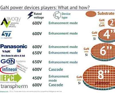 growing demand for wireless EV chargers. Hospitals have already started using robots with GaN components to improve efficiency and productivity. Scanners and nerve-muscle simulators are increasingly using GaN-based semiconductor components to increase their positioning capabilities. In the future, this technology is expected to replace silicon in medical equipment and devices.
As the telecommunications sector expands, the need for energy-efficient GaN devices is rising. The increasing number of consumers wants fast, reliable Internet access, and this is driving the demand for such devices. However, the high cost of maintenance is a hindrance in the growth of this market. Therefore, manufacturers are focusing on developing new applications for this material. The market for gallium nitride devices is set to grow at a rapid pace.
The growth of the market for gallium nitride semiconductor devices is expected to continue. As the number of robots using GaN components grows, hospitals are relying on this technology for increased efficiency. Many nerve-muscle simulators and other medical equipment will soon use GaN semiconductor components to ensure accuracy. This is why this material is an excellent replacement for silicon in these applications.
With its versatility, gallium nitride devices are a key part of the electronics industry. They are ideally suited for high-power transistors and high-temperature operation. Furthermore, GaN-based semiconductors are increasingly used in wireless EV charging. This technology is set to eventually replace silicon in all kinds of medical equipment, including nerve-muscle simulators and diagnostic equipment.
As the global demand for EVs continues to grow, the global market for gallium nitride devices will grow at an estimated 5.2% CAGR over the next five years. In addition, this technology is expected to replace silicon in medical equipment and nerve-muscle simulators. Its broad range of applications will increase its competitiveness in these markets. So, who sells gallium nitride?
With the expansion of the telecommunications industry, demand for energy-efficient GaN devices is expected to grow dramatically in the coming years. In particular, hospitals will be using robots with GaN-based components to help them diagnose and treat patients. In addition, scanning equipment based on this technology is expected to replace silicon in the next few years. It will also replace silicon in nerve-muscle simulators.
The global market for gallium nitride devices is set to grow at a 5.2% CAGR during the next five years, according to a study by Fortune Business Insights. The study breaks down the market by type, wafer size, and end user. Some of the major applications for this technology are medical devices, sensors, and fast chargers. The growing demand for these products will drive the global market for gallium nitridiride.
Increasing demand for energy-efficient GaN devices has led to the development of smart wireless chargers. The device market for the semiconductors using this technology is set to grow at a 5.2% CAGR over the next five years, as the growing demand for fast chargers in the healthcare industry is fueling the growth of the industry. The technology is widely used in wireless EV charging and is set to become a staple in the world's electrical and electronics industries.
While silicon-based semiconductors have dominated the market since the 1990s, gallium nitride is rapidly replacing its silicon counterparts. Moreover, because of its superior properties in optoelectronic applications, gaN is being used in a wide range of electronic products. For example, a GaN-based solar cell array has low
Is GaN Better Than Silicon?
The answer to the question, "Is GaN better than silicon?" depends on your specific application. In some applications, silicon is better because of its long history of reliability, and in others, GaN is superior because it requires less physical space and less power to operate. Its small size and high-temperature operation make it ideal for fast charging technology. But what are the advantages of using GaN over silicone? We've outlined the top three benefits below.
Switching losses are an important consideration when choosing a semiconductor material. While it's true that silicon is cheaper, it's worth remembering that its manufacturing methods are well-established. While it's true that silicon is a popular material, GaN is significantly more expensive. But if you're looking for a fast-charging battery, GaN could be the perfect solution. It can also be used in other types of electronic components, including mobile phones and other electronic gadgets.
One major advantage of GaN over silicon is that it can handle higher voltages and consume less power. This is a major advantage of GaN over silicon in many applications. Moreover, GaN can be produced more cheaply than silicon. The downside of this material is that it's less flexible than the semiconductor material. So, it's better to choose GaN over the cheaper alternative. Aside from being cheaper than its silicon counterpart, it is easier to produce than a semiconductor made of silicon.
GaN is faster than silicon, which means it can switch at higher frequencies. This leads to smaller and more powerful devices. It also has a wider band gap, making it more efficient than silicon. But the biggest disadvantage of GaN over its silicon rival is its cost. The cost of GaN wafers is still not competitive with those of the same size made with silicon. That is why it is still more expensive than silicon.
GaN is a more flexible semiconductor. Its advantages are not limited to automotive applications. In addition to LEDs and blue lasers, GaN is also a great choice for power conversion schemes in motor drives and hybrids. Despite its relatively high cost, it is still better than silicon in many applications, and the latter is increasingly becoming the standard in a variety of industries. You can even get a broader range of uses for GaN in the electronics industry.
Despite being inferior to silicon, GaN is superior to its silicon cousin in terms of power efficiency. Its lower temperature and high voltage allow GaN to be smaller and consume less power. As a result, GaN transistors are also more efficient than their equivalents in the semiconductor market, which makes them an excellent candidate for 5G base stations. If you're wondering if it's worth buying GaN-based electronics, you've come to the right place.
As far as comparing GaN and silicon, it's important to consider the long-term cost savings potential. When it comes to LEDs, GaN's high-power-density semiconductors have a higher melting point than their silicon counterparts. However, they have a higher price tag than their silicon counterparts. So, if you're looking for a better LED, GaN is the way to go.
As a semiconductor device, GaN has many advantages over silicon. Its high-power density and low-temperature resistance make it a more efficient choice for high-speed devices. Its high dimensional stability makes it ideal for optoelectronic applications. Its high-frequency characteristics make it a superior choice for microwave components. Besides, its comparatively higher price points make GaN more flexible.
In the semiconductor industry, GaN technology is used in the manufacturing of white and blue LEDs. Its advantages over silicon are the same. Since silicon is a cheaper and more efficient semiconductor material, it can be more easily integrated into electronics. Among the benefits of GaN is its high-performance capability. It is compatible with many semiconductors and can be found in a wide range of applications. It can be a useful alternative for many applications, particularly for wireless devices.
In contrast to silicon, Gallium nitride has a higher critical electric field strength. While silicon has a lower breakdown voltage, GaN has higher electron mobility. Its high electron mobility makes it more advantageous for high-power products. In addition, it offers fast switching speeds and good reverse-recovery performance. All of these are important in power applications. If you're considering whether to use silicon or GaN, consider the advantages of both materials.
How Do You Make Gallium Nitride?
There are several ways to make gallium nitride, a new wonder material that may be used to power Google and even help detect skin cancer. The technology could also improve battery capacity and help to create smaller, more powerful electronics. If the research is successful, it could also be used to make the power adaptors for the next generation of electric vehicles. The science behind the process is fairly straightforward, and Professor Rachel Oliver of the Cambridge Centre for Gallium Nitride says it's easy to do.
Gallium nitride is a binary III/V semiconductor with a high melting point. Because it's suitable for semiconductors, it's often grown on sapphire crystals. However, it's important to note that sapphire is not as crystalline as gallium nitride. This is because sapphire is a much better source of oxygen than gallium nitride, which causes dislocations.
One of the main uses for gallium nitride is in optoelectronics. Because it has a wide bandgap, this substance is perfect for high-power, high-frequency, and high-frequency electronic applications. In fact, the technology behind LEDs is based on gallium nitride. With its broad bandgap, it makes for a great semiconductor for these applications.
Gallium nitride is a low-efficiency compound with a wide bandgap. The main advantage of gallium nitride is that it is a great choice for high-frequency and high-power applications. Because of its wide bandgap, it's an excellent choice for optoelectronic and high-frequency devices. The process also yields low-cost semiconductors.
Gallium nitride has an extremely wide bandgap, which is an important feature for LEDs. It can handle a wide range of temperatures and is resistant to ionising radiation. It is much less expensive to produce than silicon, which made it popular in consumer electronics. Its properties are similar to those of silicon, but it is less reactive. The process for making gallium nitride is much more complex and time-consuming than that of silicon.
The process for making gallium nitride is based on the Wurtzite crystal structure. Sapphire crystals are more commonly used than gallium nitride, and it is important to understand why the latter is advantageous. Quartz, for example, contains more gallium than any other semiconductor, and its wide bandgap makes it a great material for optoelectronic applications.
Gallium nitride is an excellent material for high-frequency and high-power applications. It is more expensive to produce than silicon, and this makes it more difficult to produce large quantities of it. The advantages of using gallium nitride include its high bandgap, which means it is compatible with many 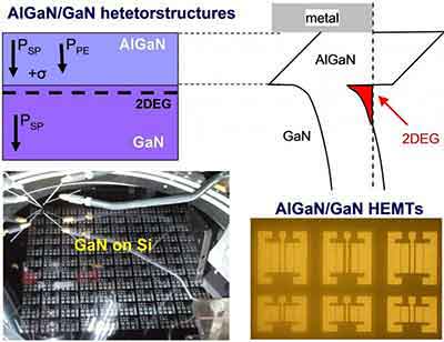 electronic devices. The bandgap is a key feature for semiconductors. Its low bandgap is important for optoelectronic devices.
Gallium nitride has a high bandgap, which means it can handle higher temperatures than silicon. Its low bandgap is one of the key advantages of gallium nitride. Besides its low bandgap, it has a wide temperature range and is resistant to ionising radiation. Therefore, it can be applied to many different types of electronic devices.
Gallium nitride is a semiconductor material that is made of gallium and nitrogen. It has a high melting point and is an excellent semiconductor material for high-power and high-frequency applications. But, while it has great potential, it has been overshadowed by silicon as a preferred material for semiconductor base materials. It is also used to power military hardware. But, what are its advantages?
Aside from being a direct bandgap semiconductor material, gallium nitride is also an important component in lighting technology. This material is a component of flat-screen LED televisions and 4GLTE cell phones. It is an excellent sensor material and is already used in a wide variety of electronic devices. And, because of its wide bandgap, it has the potential to handle a wide range of voltages.
Gallium nitride is an exceptional material with an enormous bandgap. The energy required to release an electron from a material's nucleus is determined by the narrow bandgap. In addition, the wide bandgap of gallium nitride makes it a very good material for use in high-power and high-frequency electronic devices. Aside from being a good semiconductor, it is also a good choice for memory in other environments.
Gallium Nitride Benefits over Silicon in RF Devices
Gallium Nitride (GaN) is a wide bandgap semiconductor material that has several advantages over traditional silicon-based materials when used in radio frequency (RF) devices. These advantages include:
-
Higher breakdown voltage: GaN-based devices can operate at much higher voltages than silicon-based devices, which allows for higher power handling capabilities.
-
Higher electron mobility: GaN has a higher electron mobility than silicon, which means that devices made from GaN can operate at higher frequencies.
-
Higher thermal conductivity: GaN has a higher thermal conductivity than silicon, which means that GaN-based devices can dissipate heat more effectively, leading to higher power densities and improved reliability.
-
Wide bandgap: GaN has a wide bandgap, which allows it to operate at higher temperatures and high frequency.
-
Low cost: GaN based devices are becoming more cost effective and competitive with Si based devices.
Overall, GaN-based RF devices are able to offer higher performance and improved reliability compared to traditional silicon-based devices. They are widely used in high-power, high-frequency applications including
- power amplifiers
- microwave and millimeter-wave circuits
- RF front-end modules for wireless communications systems.


![]()


 material for semiconductors in high-temperature settings. It also accepts magnesium, making it a p-type semiconductor. It can be synthesized from pure gallium and ammonia. The combination of these two materials, heat, and pressure, results in a solid material.
 growing demand for wireless EV chargers. Hospitals have already started using robots with GaN components to improve efficiency and productivity. Scanners and nerve-muscle simulators are increasingly using GaN-based semiconductor components to increase their positioning capabilities. In the future, this technology is expected to replace silicon in medical equipment and devices.
 electronic devices. The bandgap is a key feature for semiconductors. Its low bandgap is important for optoelectronic devices.