We need GaAs Wafers 100 um thickness if this cannot be achieved then as thin as thin as possible. Diameter 1 inch - 1.15 inch. We would prefer if the wafers are support free—not on a metal support. I’m not sure if you have to polish the wafers on both sides to achieve the thickness but it is not it is not necessary for us to have the wafers polished. If it is easier for you not to polish then don’t worry about it.
These foils will not be used for semiconductor – we will use them for cross section measurements in our proton beam.
Gallium Arsenide (GaAs) Wafers for Research/Production
Why is Gallium Arsenide Better Than Silicon?
How we help researchers:
For specs and pricing reference #210847.
Problem: Cell phones are amazing, but they have a few big problems. First, they take up a lot of space. Second, they don't last very long on battery power.
We all know that we need to be connected all the time, but our cell phones just can't keep up with our busy lives. They run out of juice too quickly and we can't always find an outlet to plug in.
Solution: Gallium arsenide is the answer to our battery woes. This material moves electrons faster while consuming less power, which means your phone will last longer on a single charge.
Get Your Quote FAST! Or, Buy GaAs Online and Start Researching Today!
Two benefits of GaAs wafers over Silicon wafers are:
1) GaAs moves electrons faster while consuming less power. Think of your cell phone. Tight spaces and short battery life. GaAs  provides a real advantage over silicon for some components.
2) GaAs has direct band-gap properties make all-optical buses direct light on-chips more efficiently than wires do on silicon.
Gallium Arsenide for X-Ray Spectroscopy
A scientist needed help sourcing a GaAs Wafer:
Our research group is looking to purchase ultrasmooth GaAs wafers for a very sensitive optical setup. Do you have a wafer that is smooth to approximately +-10 nanometers with warp of the wafer below 100 nm across 5 mm. Essentially two of these wafers must have an unobstructed space across 5 mm if they are separated by a 200 nm gap. This wafer will be cut into multiple 5x10 mm segments so a 2'' diameter should suffice. Please let me know if you have any products that could work for us. If you do have a product could you send a quote as well.
We are using this for x-ray spectroscopy. We're essentially redoing an experiment but with a way more flat material.
UniversityWafer, Inc. Quoted:
GaAs Item #1299
100mm Undoped <100> 1E7 625um DSP Prime Grade EPD (Average): less than or equal to 5,000, Doping: Semi-Insulating
Gallium Arsenide VGF and LEC Grown
We have Gallium Arsenide Wafers (GaAs) III-V direct band gap semiconductor that are both the commonly used Vertical Gradient Freeze (VGF) and also Liquid encapsulated Czochralski (LEC) grown high-purity single crystal that are semi-insulating.
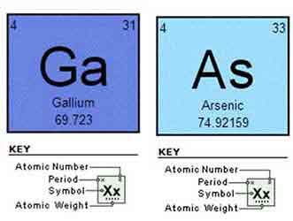
Gallium & Arsenide Symbol
Recently a researcher inquired about 150mm Gallium Arsenide with Chromium (Cr) doping.
Client request:
We are biding projects demanding around 20 pcs chromium-doped 6" GaAs wafers and 5~10pcs 4" Silicon-on-Sapphire(SOS) wafers. Can you offer these items?If yes, I will send you detailed specification.
Our Reply:
We do have the technology and equipment to make SI GaAs:Cr even in 150mm diameter.
How? A new crystal ingot would have to be grown and then sliced and polished into wafers. With Ro>1E8 Ohmcm, mobility >5,000cm²/Vs is unattainable, but we can probably reach u>4,000²/Vs. Likewise EPD<500/cm² is unrealistic for LEC process, but we can certainly achieve 5E4/cm². To dope with Chromium, we have to use the LEC rather than the VGF process.
We also quoted:
Semi-Insulating undoped Gallium Arsenide wafers, P/P
6"Ø×625±25µm,
VGF SI GaAs:-[100 -2.0±0.5º towards <001>]±0.5°, Ro=(1.2-1.7)E8 Ohmcm, Both-sides-polished (Epi-Ready), Bow/Warp<30µm, Diameter 150.0±1.0mm, SEMI Notch @ (010)±5º, 1.0±0.25mm deep, {Mobility<5,000, EPD<500} crystal structures
Nickel Arsenide
Researchers also ask us if we carry Nickel Arsenide. We do. Please send us your specs.
Arsenic FYI
Arsenic atoms have 33 electrons and 33 protons with five valence electrons.
What Glass Bonds to Gallium Arsenide?
A researcher looking for glass (or quartz) wafers that is used for bonding to GaAs wafers. Below are the basic requirement:
- The glass wafer must be transparent at wavelength of 940nm
- Wafer diameter: 4 inch
- 3. Wafer thickness: ~500um
- 4. Coefficient of thermal expansion (CTE) is as close to CTE of GaAs (5.73 ppm/K) as possible.
- 5. Double side polished.
CTE of GaAs is 5.73 ppm/K = 5.73x10^-6 /K. So the CTE of the JGS2 Fused Silica is an order of magnitude lower than that of GaAs.
I think in general CTE of quartz/fused silica is too low, while CTE of standard glass like BK7 is too high. Do you have something that may fit our purpose?
Solution:
We find that Corning 7056 or 7052 seem to be good options. Please send quantity for an immediate quote.
Gallium Arsenide to Make Laser Diodes
 How to Make Laser Diodes with Gallium Arsenide is the subject of an interesting new book. It is a very straightforward process that uses a single semiconductor material - gallium arcsenide. Using the compound, you can make the laser diodes that light up. The key is in making the materials work together in a way that allows them to be both effective and efficient.
A gallium arcsenide laser has a similar construction to a light emitting diode. It is a semiconductor that produces both coherent and incoherent light. These lasers are made up of two doped layers of gallium arcsenide, one of which is an n-type semiconductor, and the other layer is a p-type semiconductor. In the process, doping agents such as silicon, aluminum, and selenium are added to create a double-layered laser.
The transition between the two layers is known as a direct bandgap. This transition occurs between a p-type layer and an n-type layer. When these layers join, they form a p-n junction, a junction that separates the two types of semiconductors. This structure also allows for high frequency operation. The process is known as ranging, and it works by sending an optical pulse to a distant reflector. The laser pulse is sent, and the return pulse is received at the same position. As the laser pulse goes out, the clock starts to a remote reflector.
Which GaAs were grown with B2O3 flux and might have a useful boron acceptor concentration?
Some of our wafers are grown by LEC and these have large Boron concentrations, and some are grown by VFG and these have little lower Boron concentrations.
Undoped Semi-Insulating GaAs tend to have lower Boron concentration than doped GaAs.
We also have some D shape wafers and small pieces of ingot of GaAs:Si that were crystallized by the HB process. This material was synthesized and then grown into crystals in quartz boats without the use of B2O3, so they are totally Boron-free (although I do not have formal GDMS measurements of their Boron concentration).
Let me know what material you require, and what Boron concentration in GaAs you can tolerate.
Let me know the type and degree of doping, weather you need wafers or crystal pieces, their size and thickness.
I am sure that we can find what you need.
Substrates Used for Metal Halide Perovskites Crystal Growth
Researchers have used the following Gallium Arsenide and Sapphire wafers for their research.
GaAs Item #3411
100mm N/Si <100> Res (1.2-9.9) x 10-3 350um SSP Surface Orientation: (100)15° off towards <111> A ±0.5°
GaAs Item #3508
100mm Undoped <100> Res 1E7 625um SSP GaAs VFG, semi-insulating, undoped, EPD: <7100 cm-2, Surface: DSP From Side: polished epi ready, Back Side: polished, Flats: US (2 flats)
Sapphire Item #2562
100mm <0001> 650um DSP C-M plane 0.2°, Double Side Polished, Micro-roughness: Ra<0.35nm, Primary flat Warp<21um, TTV<16um
Metal halides perovskites, such as hybrid organic–inorganic CH3NH3PbI3, are newcomer optoelectronic materials that have attracted enormous attention as solution-deposited absorbing layers in solar cells with power conversion efficiencies reaching 20%. Herein we demonstrate a new avenue for halide perovskites by designing highly luminescent perovskite-based colloidal quantum dot materials. We have synthesized monodisperse colloidal nanocubes (4–15 nm edge lengths) of fully inorganic cesium lead halide perovskites (CsPbX3, X = Cl, Br, and I or mixed halide systems Cl/Br and Br/I) using inexpensive commercial precursors. Through compositional modulations and quantum size-effects, the bandgap energies and emission spectra are readily tunable over the entire visible spectral region of 410–700 nm.
Gallium Arsenide (GaAs) Wafers for Testing X-ray Detector
Scientist asks:
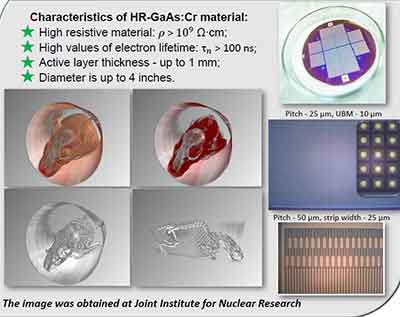
I am looking for some special GaAs wafers for testing x-ray detector, something like described in this link. I notice that your site has chromium doped GaAs and it seems that they also have high resistivity, which is good. Do you have more information on your GaAs:Cr? Like what kind of growth method? How the Cr dopants were added?
UniversityWafer, Inc. Quoted:
| Item | Typ/Dop | Orient. | Diam. | Thck (um) | Pol | Res Ωcm | Nc a/cm3 | Mobil cm2/Vs | EPD /cm2 |
| Cr doped, EJ Flats, Epi Ready, 4 of 7 have edge chips | |||||||||
| 2186T | SI GaAs:Cr | [100] | 2" | 1,500 | SSP | 1.05E8-1.28E8 | 2,246-4,334 | <3.3E4 | |
| Cr doped, EJ Flats, Epi Ready | |||||||||
| 7336 | SI GaAs:Cr | [100] | 2" | 400 | DSP | 1.05E8-1.15E8 | (1.3-1.4)E8 | 2,246-4,334 | <4E4 |
What is Gallium Arsenide's Etch Pitch Density Spec?
The etch pitch density of a GaAs/Si substrate is about 2 x 10 8 cm2 and the etch pitch density for a GaAs/OI substrate is 5x10⁻⁷ cm2 and 3x10⁻⁶ cm2. Thus, the reduced EPD of the GaAs layer indicates improved crystal quality. And despite these limitations, the method is highly accurate and useful for calculating the etch pitch density of large crystals.
Why is Gallium Arsenide So Expensive?
Silicon and gallium arsenide are two of the most widely used semiconductors in the world, and both are very expensive. But the process of creating these materials is actually quite simple. First, semiconductor manufacturers form the raw crystals into wafers, which are circular platters made of highly purified material. Then, they go through a series of manufacturing steps to create computer chips, solar cells, and other electronic devices. However, a single 8-inch diameter silicon wafer will cost $5, while an 8-inch-diameter gallium arsenide wafer can cost $5,000.
In order to manufacture solar panels with a gallium-arsenide layer, researchers need a $5,000 silicon wafer. The silicon wafer is only a backing for the device and is inconsequential. After the gallium arsenide material flows across the wafer, it condenses into a thin layer of circuitry. The wafer is only needed for backing purposes.
Since gallium arsenide is more expensive than silicon, it is only practical in very niche applications. But it can be used in a variety of applications, including solar panels and cellphones. Stanford researchers have invented a manufacturing process to make these devices. This technology could make these semiconductors useful for solar panels. If it can be made affordable for the average consumer, it will become the most common choice for most home solar panel makers.
Video: Gallium Arsenide vs Silicon
Gallium Arsenide LIDAR Application
Gallium Arsenide (GaAs) substrates play a crucial role in LiDAR (Light Detection and Ranging) technology due to their unique physical and electronic properties. Here's a breakdown of their function:
-
High Electron Mobility: Gallium Arsenide has a high electron mobility compared to silicon, which allows for faster signal processing speeds. In LiDAR systems, it's super critical to quickly handle the bouncing back light signals for real-time mapping and spotting things on the fly.
-
Direct Bandgap Material: GaAs is a direct bandgap semiconductor. Because of its unique qualities, GaAs is super good at both shooting out light and taking it in. In LiDAR systems, this translates to more efficient laser diodes for emitting the light pulses and better photodetectors for receiving the reflected signals.
-
Temperature Stability: GaAs substrates maintain their performance over a wider range of temperatures compared to silicon. Because the LiDAR system needs to work well in different temperatures, especially in cars and outdoors, having a stable material like gallium arsenide is really important.
-
Because the material works well at higher frequencies, it's useful for precise, high-resolution LiDAR imaging. The material's ability to operate effectively at higher frequencies makes it suitable for LiDAR applications that require high-resolution imaging and precise distance measurements.
-
Resistance to Radiation: Gallium Arsenide is more resistant to radiation damage than silicon, which is beneficial for LiDAR systems used in space exploration or in high-radiation environments.
To put it simply, LiDAR systems just work better with Gallium Arsenide - they're quicker, more efficient and reliable, and tougher too; this makes them perfect for anything from self-driving cars to creating maps.
Growing LT-GaAs ForPhotoconductive Antenna Fabrication
A PhD candidate requested the following quote:
We need LT-GaAs film grown on undoped GaAs substrate. This is for photoconductive antenna fabrication. Here are a few requirements: LT-GaAs film is 0.5um, and should be grown in low temperature like 250℃. The substrate is 350um GaAs with 20mm diameter wafer (just like we discussed before). The quantity is planned to be 5 but we are going to buy ONE to test if fabrication goes well then we will buy more. If you may, please tell me the temperature and the time of the growth, and the temperature and the time of annealing (we need to mention the wafer provider and the process of wafer fabrication in the paper). Looking forward to your reply!
Reference #278017 for specs and pricing.
Leading Supplier of Gallium Arsenide wafers up to 150mm in diameter. Below are just a small sample of Gallium Arsenide SALE!
GaIlium Arsenide (GaAs) wafers wide band gap has benefits that silicon lacks. GaAs applications include:
- Optoelectronic
- High-power
- High-frequency devices
Who Makes Gallium Arsenide Wafers?
UniversityWafer, Inc. provides all specs of GaAs wafers including Undoped Semi-Insulating Epi Ready EJ & US Flats GaAs. Contact us for a quote! More specs are in stock. Please ask for the list.
| Item | Typ/Dop | Ori | Dia | Thck(μm) | Pol | ResΩcm | Nca/cm3 | Mobil cm2/Vs | EPD/cm2 |
| 6093 | undoped SI | [100] | 2" | 380 | P/E | n-type 9.67E7 | 1.15E+07 | 5,590 | <7E4 |
| H093 | undoped SI | [100] | 2" | 500 | P/E | n-type 9.5E7 | 1.20E+07 | 5,360 | <6E4 |
| 5628 | undoped SI | [310] ±0.5° | 2" | 400 | P/E | n-type 5.5E7 | 1.90E+07 | 5,800 | <1,400 |
| 6814 | undoped SI | [100] | 2" | 1,000 | P/P | n-type 1.18E8 | 1.45E+07 | 3,656 | <4.5E4 |
| 2295A | undoped SI | [100-4° towards[111A]] ±0.5° | 51.3mm | 380 | P/E | n-type 7.4E7 | 1.70E+07 | 5,000 | <8E4 |
| 2237 | undoped SI | [100] | 2" | 6,700 | P/P | n-type 1.1E8 | 1.10E+07 | 5,000 | <1E5 |
| 2328C | undoped SI | [100] | 2" | 5,000 | P/E | n-type 4E7 | 2.70E+07 | 5,700 | <5.3E4 |
| 2313 | undoped SI | [110] | 2" | 500 | P/P | n-type | (3.2-11)E7 | 3,700-4,400 | <6,000 |
| (1.9-4.4)E7 | |||||||||
| 2308B | undoped SI | [310] ±0.5° | 2" | 400 | P/E | n-type 5.5E7 | 1.90E+07 | 5,800 | <1,400 |
N-Type Silicon Doped GaAs
| Item | Typ/Dop | Ori | Dia | Thck(μm) | Pol | ResΩcm | Nca/cm3 | Mobil cm2/Vs | EPD/cm2 |
| 3F051 | N/Si | [100-2° towards[011]] | 2" | 350 | P/E | (0.91-1.36)E18 | <2,500 | ||
| 7256 | N/Si | [100] | 4" | 625 | P/E | (3-8)E17 | <10,000 | ||
| E876 | N/Si | [100-15° towards[111A]] ±0.5° | 4" | 350 ±20μm | P/E | (0.4-4.0) | >1,000 | <5,000 | |
| E18 | |||||||||
| 6418 | N/Si | [100-2.0° towards[110]] ±0.5° | 4" | 350 | P/E | 0.0012-0.0099 | (2-4)E18 | 1,500-2,500 | <3,000 |
| 7175 | N/Si | [100] ±0.25° | 2" | 450 ±10 | P/E | <0.1 | (5-100)E16 | >1,000 | <8,000 |
| K220 | N/Si | [100] | 2" | 350 | P/E | (8.8-10.4)E17 |
P-Type Zinc (Zn) Doped GaAs
| Item | Typ/Dop | Ori | Dia | Thck(μm) | Pol | ResΩcm | Nca/cm3 | Mobil cm2/Vs | EPD/cm2 |
| 7151 | P/Zn | [100] ±0.25° | 4" | 450 | P/E | <7E-3 | (3.1-4.2) | >81 | <10,000 |
| E19 | |||||||||
| 5490 | P/Zn | [100] | 2" | 400 | P/E | 1.3-420.0 | (9-29)E15 | 47-163 | <5E4 |
| 6165 | P/Zn | [100] | 2" | 300 | P/P | 1.81 | 2.46E+16 | 140 | <5E4 |
| L220 | P/Zn | [100] | 2" | 350 | P/E | (1-3.08)E17 | |||
| D175 | P/Zn | [100] ±0.25° | 2" | 450 ±10 | P/E | (8-30)E18 | <8,000 | ||
| H180 | P/Zn | [100-6° towards[110]] ±0.5° | 2" | 350 | P/E | 0.0030 - 0.0065 | (1.0-2.7) | 75-84 | <1,906 |
| E19 | |||||||||
| 6272 | P/Zn | [111B] ±0.5° | 2" | 300 | P/E | 0.10-0.12 | (2.8-3.0) | 193-208 | <5.7E4 |
| E17 |
Chromium (Cr) Doped GaAs
| Item | Typ/Dop | Ori | Dia | Thck(μm) | Pol | ResΩcm | Nca/cm3 | Mobil cm2/Vs | EPD/cm2 |
| T3911 | SI GaAs:Cr | [100] | 4" | 625 | P/P | >1E7 | |||
| 7336 | SI GaAs:Cr | [100] | 2" | 400 | P/P | 1.05E8-1.15E8 | (1.3-1.4)E8 | 2,246-4,334 | <4E4 |
N-Type Tellerium (Te) Doped GaAs Substrate
| Item | Typ/Dop | Ori | Dia | Thck(μm) | Pol | ResΩcm | Nca/cm3 | Mobil cm2/Vs | EPD/cm2 |
| 6974 | N/Te | [111] ±0.5° | 1" | 500 | P/P | 0.00245 | 8.21E+17 | 3,101 | <5E4 |
| T3686 | N/Te | [100] | 4" | 750 | P/P | (3.6-17.0) | |||
| E16 |
GaAs Wafers to Develop Fabrication Processes
A researcher requested a quote for epitaxy ready (100) undoped (semi-insulating) GaAs 2” wafers with one side polished. Would it be possible to have a quote for 10 substrates?
UniversityWafer, Inc. Quoted:
| Item | Material | Orient. | Diam. | Thck (μm) |
Surf. | Resistivity Ωcm |
Nc a/cm3 |
Mobil cm2/Vs |
EPD /cm2 |
Comment |
|---|---|---|---|---|---|---|---|---|---|---|
| 7175 | n-type GaAs:Si | [100] ±0.25° | 2" | 450 ±10 | SSP | <0.1 | (5-100)E16 | >1,000 | <8,000 | VGF; EJ Flats; Epi Ready |
| J180 | undoped SI GaAs:- | N/A |
2" | 350 | P | n-type | N/A | N/A |
N/A |
SEMI TEST (shallow pits), NO Flats; Epi Ready, Group of 5 wafers |
Below are some applications that GaAs wafer benefits

 The Gallium Arsenide Hall Effect Sensor is a semiconductor device that measures the mobility of electrons. Its final output voltage depends on the temperature, and is characterized by a red line cross-shape. At -40 deg C, the highest measured Hall voltage is V H = 72.5 mV. As the temperature increases, the output signal decreases, because increased temperature causes carrier scattering. As the temperature rises, the mobility of carriers of the Hall sensor decreases, resulting in a lower output signal.
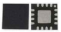 conduct electricity more efficiently than silicon, which makes it an excellent candidate for fast-switching devices. Other benefits of gallium arsenide include its resistance to heat and radiation, making it a great material for LEDs. Lastly, it can give off light. For this reason, it is a desirable material for LEDs.
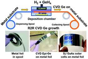 The materials in gallium arsenide are much more effective than those made from silicon and other common materials. These panels also have the best performance of all the types, but their price tag can make them out of reach for many people. That said, as technology continues to improve, it is likely that solar panels will become more affordable for the average homeowner. And even though the prices of solar panels are expected to go down in the future, the material that makes them so effective has a long history of use in semiconductors.
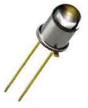 This light has a short wavelength of 850nm to 940nm. An electrical current flows through the junction, producing light. As the electrical current increases, so does the light output. These diodes are often used as night lights, and the technology has several applications.
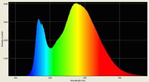 amounts of infrared radiation in the 850 to 900 nm wavelengths. During manufacturing, a forward current flows through the junction of the two materials, allowing them to produce light. This type of LED has a high light output, but is not a good option for outdoor lighting.