Graphene Under AFM Observations for Research
Get Your Quote FAST!
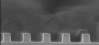
Silicon Wafer Grating
Below is an image of what wafer grating looks like.
Graphene Under Atomic Force Microscopy (AFM) Observations
We provide the silicon wafers you need to observe the Graphene.
Clients have used the following silicon wafer with great success:
Si Item #444 -50.8mm P/B <100> 0-100 320-350um SSP Test Grade
Below is a typical question and answer between researcher and us:
We need detailed specification to determine initial costs for the project and costs per wafer.
[Q1] Can you give us more details regarding your request?
[Q2] What kind of pattern do you need?
[Q3] Which dimensions and tolerances?
[Q4] Depth of structures?
[Q5] How many wafers do you need and how often?
At this feature size we have mask reticles which we step over the wafer. Per reticle CD structures are necessary.
I hope this is not a problem.
Researcher Reply
A1: In our experiment, we need the period of the feature less than 200nm. (i.e. ridge width + valley width <= 200 nm)
A2: Currently, periodic line pattern is enough for initial study.
A3: Dimension of the wafer should be at least 10mm * 10mm.
A4: Depth of the pattern is not important. 10nm ~ 100 nm is good.
A5: It depends on the price and the quality of the wafer. For the initial experiment, we don't need much (may be around 10). After successful attempt, we may need much more.