Indium Gallium Arsenide (InGaAs) Wafers for Research
Indium Gallium Arsenide Wafers In Stock
InGaAs is a high-mobility semiconductor that promises to increase a transistor's performance for high-frequency applications.
Get your InGaAs quote FAST! Guaranteed!
Indium Gallium Arsenide Applications
Indium gallium arsenide (InGaAs) is a material that is often used in the production of semiconductor devices. It has a number of advantageous properties that make it useful in a variety of applications, including:
-
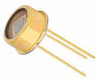
Photodetectors: InGaAs is highly sensitive to certain wavelengths of light, making it an ideal material for use in photodetectors. It is often used in applications such as fiber optic communication systems and infrared cameras.
-
Solar cells: InGaAs is also used in the production of solar cells, particularly in concentrator photovoltaic systems that use lenses to focus sunlight onto a small area of photovoltaic material.
-
High-speed electronics: InGaAs has a high electron mobility, making it useful in the production of high-speed electronic devices such as transistors and integrated circuits. It is often used in applications that require high-frequency operation, such as in radar systems and high-speed data transmission.
-
Medical imaging: InGaAs is used in the production of medical imaging devices such as CT scanners and PET scanners, which use radiation to create images of the inside of the body.
-
Military and aerospace: InGaAs is also used in a variety of military and aerospace applications, including in the production of sensors and electronics for use in aircraft and missiles.
Overall, the main advantage of InGaAs is its ability to operate at high speeds and in a wide range of wavelengths, making it useful in a variety of applications that require these capabilities.
Photodetectors
Commonly used to measure optical power in the near IR (NIR) range.

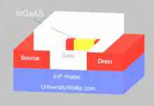
Transistors

We sell the InGaAs and InP Substrates. One concern with growing InGaAs on silicon is lattice mismatch. Our engineers may be able to help yu in this regard. Please email us today.
InGaAs for Thermophotovoltaic Application
A researchers asked the following:
I would like to order 2 wafers of InGaAs epifilm with complete structure as shown: ingaas.png Kindly note that this is a full structure all grown on an InP substrate. I would need the following information from you:
- The quote for the proposed structure
- Delivery time
- Method of payment
- What is the test of quality?
UniversityWafer, Inc. quoted and the researcher purchased:
$Contact Us, based on 2pcs. Reference RFQ#262172
Remark:
1/ P-InGaAs or p-InP is doped by Mg or Zn, rather than Be.
2/ substrate is 350um.
What is Indium Gallium Arsenide (InGaAs)?
Indium Gallium Arsenide is a common chemical element that can be used in various applications. This article will discuss what this substance is, its uses, and how it affects the market. It will also help companies understand the potential of this material. The report will give you a clear picture of the Indium Gallium Arsenide market and the competitive landscape. This report includes both historical and future data for Indium Galvanide, and will help you strategize your next move.
The research report analyzes the current state of the Indium Gallium Arsenide market and future prospects. It presents data from 2016 to 2020 as well as a seven-year forecast up to 2028. The study includes sales data and revenue, and analysis of the different end-use industries for this material. You can also view the entire report and see a comparison chart of the current market size and potential growth.
This research report includes historical and forecast data for the Indium Gallium Arsenide market. This market report analyzes regional and country-level trends for the Indium Gallium Ansenide industry. It also provides insights into the key players and trends that are influencing the market. The research report is free to download and contains comprehensive tables and figures. The full report is available at the link below.
The report covers the positive and negative market dynamics for the Indium Gallium Arsenide market. It also provides the current market size, revenue, and trends. You can also get a clearer idea of the competitive landscape. The market will be more dynamic with the latest advances in technology. The key players in the industry are listed below. For more information, please visit the Indium Galvanized Arsenide Market
The Indium Gallium Ansenide market is highly dynamic and has positive and negative dynamics. Its overall growth is largely affected by the COVID-19 pandemic and will experience a slowdown or increase in price, and will experience a slowdown or a complete stop in production. The global Indium Gallium Ansenide market will show a sharp rise in prices in the coming years, and will remain a valuable component in solar panels and detectors.
Despite the high level of innovation in solar panels, indium gallium anodide is a common chemical. The indium gallium anodide market is characterized by rapid growth. Several factors affect the Indium Gallium Ansenide market. A significant one is the lack of available materials in many industries. It is a major source of energy in the solar sector. There are a number of benefits to using this material for these applications.
The Indium Gallium Ansenide market is expected to grow steadily over the next few years. It is widely used in optics and microelectronics. Indium is also used in thin films in solar cells. Its name derives from Latin word indicum, which means violet. As with most other semiconductors, indium is a relatively inexpensive material to purchase. However, it does have some disadvantages.
Moreover, the global Indium Gallium Ansenide market is characterized by high demand for this metal. The market for this metal has a wide range of uses, from medical devices to cellular phones. It is also an important source of fuel for solar panels. It is resistant to corrosion and is highly resistant to shock. It is an excellent choice for solar panels. If you are looking for a new source of energy, it is essential to check the Indium Gallium Ansenide market first.
The market for Indium Gallium Ansenide is highly competitive and is expected to grow over the next few years. The advantages and disadvantages of Indium Gallium Ansenide are clear, but the market is not booming yet. Rather, it is in the early stages of development. This mineral is used in a variety of products and is available in a wide variety of forms.
Indium Gallium Ansenide is a common element. It is a metal in the same family as gallium. It is found in several minerals, such as arsenolite, or loellingite and realgar. These metals have many electronic and semiconductor uses. The ternary composition of these two metals makes them ideal for use in semiconductors. The chemical name Indium Ansenide is an alloy of indium and gallium.
Indium Gallium Arsenide (InGaAs) to Fabricate PN Junction Diode
I was wondering if you had InGaAs wafers. (In:Ga ratio 53:47) I need thick layers for my application, so the thickness needs to be thicker than 50 microns. Also, would it be possible to know which materials are available as wafers? (several hundred microns thick) I am looking for thick semiconducting materials for a detector application, but I want to also base my material choice on its availability. Please let me know.
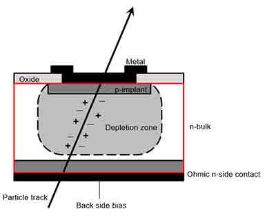
It would be great if you could recommend to me the material, after I explain what the purpose of my device is. I am trying to create a structure like the image below:
InGaAs pn Junction Diode
It is a pn junction diode, which I plan to operate under reverse bias.
This is to create and collect charges as charged particles travel through the depletion zone. (My device is a particle detector)

A university researcher asked the following:
I am wondering if the parts marked in red could be purchased from University wafer.
The material needs to be an n-type, with a window of p-type implant on the top surface.
I am planning to deposit metal on both top and bottom for electrodes, so it would be nice if the bottom layer has a material suitable for forming ohmic contact with metals. (the electrodes will probably be Cu/Au or Ti/Au).
The thickness of the bulk layer should be hundreds of microns, which I think is achievable with wafers.
Can you give me a list of wafers from the inventory which this setup would be possible?
After that, I can pick a suitable wafer from the list.
UniversityWafer, Inc. Quoted Replied:
I am not aware of any facility that grows bulk crystals of In(0.53)Ga(0.47)As alloy from which one could make wafers 50, or 100, or 350µm thick.
On the other hand, it is common to grow an Epi layer or layers of In(0.53)Ga(0.47)As on InP wafers (since the lattices match).
It is entirely common to grow a Zn doped p-type InGaAs on top of a Si doped n-type InGaAs layer.
However, in most such cases, the total InGaAs layer is about 1µm thick.
In theory, it is possible to grow a 40µm thick layer of InGaAs on an InP substrate. However, most such growth is done by the MOCVD process and this process gets very expensive for very thick InGaAs layers. However, if your budget can support it then we can make such wafers for you.
A characteristic of the MOCVD process is that it allows one to create very sharp transitions between n-type and p-type regions.
We shall try to offer the following:
Item Qty. Description
HD68. 2/10 Epi wafers, 2"Ø×350±25µm
Substrate: SI InP:Fe[100]±0.5°, Ro > 1E7 Ohmcm,
One-side-polished, back-side Alkaline etched,
Epi Layer 1: 40µm thinck, n-type In(0.53)Ga(0.47)As layer, Si doped, Nc=1E17/cc,
Epi Layer 2: 0.5µm thick, p-type In(0.53)Ga(0.47)As layer, Zn doped, Nc=1E18/cc
We are working on this RFQ, we should have a quote in a few days.
Please verify that this is what you need. We can offer double-side polished substrates and possibly substrates doped differently. We can offer different levels of doping and different thicknesses of the p-type layer.
I shall try to give you an idea of the incremental cost of the InGaAs layer thickness.
InGaAs Research Questions
A research client from a large semiconductor equipment manufacturer was interested in our InGaAs wafers.
Can you give me quotes on the 2" InGaAs wafers for the items below? 1. bare wafers, qty=10 to 100 2. Epi: Lattice matched n-type InGaAs:Si[100]±0.5°, thickness: 1.0um(±20%), Nc=1E17/cc, qty=10 to 100 3. InP/InGaAs/InP Epi wafers, qty=10 to 100
UniversityWafer, Inc. asked the following Questions.
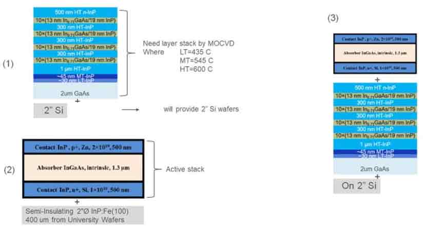
You want me to quote the three structures shown in the image below? Material Stack. Is that correct?
Regarding (1)
a. Semi-Insulating InP - that is to be 2"Ø InP:Fe(100) substrate wafer and it is to be 400µm {not 400nm} thick. Is that correct?
b. 150nm InP layer - that is to be n-type InP:Si, Nc=(3-8)E18/cc. Is that correct ?
c. 850nm InGaAs layer - that is undoped, lattice matched In(0.53)Ga(0.47)As - Is that correct ?
d. 160nm GaAsSb layer - that is p-type (Zn doped), lattice matched GaAs(0.51)Sb(0.49):Zn - is that correct?
Nc=2E10/cc is unrealistic, if you want p+ then perhaps (3-8)E18/cc or even (1-3)E19/cc is reasonable - please decide
Regarding (2)
a. Semi-Insulating InP - that is to be 2"Ø InP:Fe(100) substrate wafer and it is to be 400µm {not 400nm} thick. Is that correct?
b. 150nm InP layer - that is to be n-type InP:Si, Nc=(3-8)E18/cc. Is that correct ?
c. 2,000nm InGaAs layer - that is undoped, lattice matched In(0.53)Ga(0.47)As - Is that correct ?
d. 160nm GaAsSb layer - that is p-type (Zn doped), lattice matched GaAs(0.51)Sb(0.49):Zn - is that correct?
Nc=2E10/cc is unrealistic, if you want p+ then perhaps (3-8)E18/cc or even (1-3)E19/cc is reasonable - please decide
Regarding (3)
a. Is the substrate to be 2"Ø Semi-Insulating GaAs:-(100), 400µm thick ?
b. The three layers, 1,600nm, 300nm and 100nm are these all undoped GaAs or should they be doped to different degrees?
What do you mean by HT
c. 10× - that is to be 10 layers of In(0.16)Ga(0.84)As, 12nm thick, interspersed with 0 layers of GaAs, 12nm thick - is that correct?
Are these to be undoped or doped to be p-type ? Do specify target Nc.
d. The 400 nm GaAs spacer - is that to be undoped ?
e. 10×- that is to be 10 layers of In(0.16)Ga(0.84)As, 12nm thick, interspersed with 0 layers of GaAs, 12nm thick - is that correct?
Are these to be undoped or doped to be n-type ? Do specify target Nc.
f. 750 nm n+ GaAs - is that to be GaAs:Si, Nc=(3-8)E18/cc ?

Please answer above to clarify what is needed.
Are you asking us to quote to make structures that you already use, or is this an experimental project/ If it is experimental then perhaps 1 wafer would be a better quantity to start with.
Do you actually need above structures or are you trying to get budgetary estimates. If these are budgetary estimates then I can give you an overall cost structure and you would not have to detail each request {for example, within broad limits the type and degree of doping has no influence on cost}.
We do want to help you any way that we can.
For your item 1:
What do you mean by "bare InGaAs" wafer?
Do you mean bulk InGaAs wafers, say 400µm thick?
What In:Ga ratio do you require?, Is it In(0.53)Ga(0.47)As or some other In;Ga ratio?
Are the wafers to be one-side-polished or double-side-polished ?
For your item 2:
What is the Epi-layer thickness? what is the Epi-layer doping?
The substrate InP wafer, is it to be Semi-Insulating or n-type Semi-Conducting?
Here is an example of such a wafer:
Item Qty. Description
GD16. 2/3/10 InGaAs:Si on InP:Fe Epi wafers,
Substrate: P/P 2"Ø×350±25µm InP:Fe[100]±0.5°, Ro>1E7 Ohmcm, EPD<1E4/cm²,
Both-sides-polished, EJ Flats (two),
EPI Layer: 0.75±0.15µm thick, n-type Lattice matched In(0.53)Ga(0.47)As:Si, Nc>2E18/cc
Note: Epi layer roughness close to one molecular layer; Some backside deposits expected.
Sealed in single wafer cassettes
Price: Depends on Qauntitiy
For your item 3
What is the IP Epi-layer thickness? what is the Epi-layer doping?
What is the InGaAs Epi-layer thickness? what is the Epi-layer doping?
The substrate InP wafer, is it to be Semi-Insulating or n-type Semi-Conducting?
Current InGaAs Inventory - Buy Online!
50.8mm Undoped (100) 350um SSP
Epi: Lattice matched n-type InGaAs:Si[100]±0.5°, thickness: 1.0um(±20%), Nc=1E17 -1E18/cc.
Sealed in individual wafer container. Substrate: 2" Indium Phosphide wafers, P/E 2"Ø×350±25µm.
Epi: Lattice matched p-type InGaAs:Zn[100]±0.5°, thickness: 1.0um(±20%),Nc=1E17 -1E18/cc.
Sealed in individual wafer container. Substrate: Indium Phosphide wafers, P/E 2"Ø×350±25µm.
50.8mm InP/InGaAs/InP Epi wafers
Substrate: Indium Phosphide wafers, P/E 2"Ř×380ą25ľm, n-type P:S[100]ą0.5°,EDP<1E4/cm2.
One-side-polished, back-side matte etched, SEMI Flats.
Epi 1: InGaAs:[100] (100nm, etching stop layer).
Epi 2: InP:[100](50nm, bonding layer).
Wafers for InGaAs Detectors
A scientist prototyping Indium Gallium Arsenide detectors. The research required that a 5 mm diameter InGaAs detector (used at 1590 nm) cost too much.
The scientist asked me to look into alternatives including potentially purchasing a full wafer or more (they expect to need about 350-400 detectors per year) and having someone cut and mount the detectors. I have no idea if this kind of thing is feasible or practical so wanted to start with the simple question of is this kind of approach at all viable? Does your company do things like this (ie. grow the wafers, and have the capability to cut and mount individual detectors)?
UniversityWafer, Inc. quoted the following:
5 mm diameter InGaAs detector (used at 1590 nm), we only offer chips:
Please contact us for pricing.
