Preparing Silicon Wafers for Reactive-Ion Etching (RIE)
Wafers for Reactive-Ion Etching
UniversityWafer, Inc carriers a large selection of carrier wafers for your RIE needs. Please ask or just send us your specs and quantity.
Get Your Quote FAST!
Preparing 100mm Silicon Carrier Wafers for RIE Etching Process
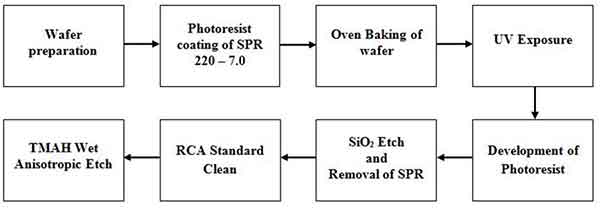
This article describes the preparation, setup, and operation of a RIE etching machine for a hundred-millimeter silicon carrier wafer. The RIE etching process consists of three major steps: wet oxidation, wet nitridation, and a wet etch step. The wet nitridation step consists of an oxidation reaction involving a solution of HBr and O2 at a flow rate of three7.5 sccm and a power level of 90 W.
 For the RIE etching process, a silicon carrier wafer of 100mm must be used. The thickness of the sample must be less than 2 mm. The resistivity of a wafer has no bearing on the transfer time. The process can last as long as the top silicon layer is present. A suitable etching time should be kept. The RIE etching machine should be equipped with a high-speed pump, a tunable laser, and a vacuum pump.
The RIE etching machine has a high rate of speed and accuracy. However, the tackiness of the etched sample can cause a number of problems. The etching machine must be able to transfer the wafer from the etching solution to the water in less than 0.6s. The RIE etching process requires a large amount of chemicals, and chemical reagents are 2 times more expensive than alkali etching. Environmental protection treatment is relatively simple.
The RIE etching machine requires 100mm silicon Carrier Wafers. The wafers must be placed on a carrier in a high-pressure chamber at four mTorr. The carrier wafer must be cooled with helium. A high iCP power level is needed to avoid over-etching. A high-pressure setting is recommended in this process.
When preparing silicon Wafers for RIE etching, the wafers must be prepared properly. The etching process should be performed at a temperature of 50 degC. This temperature must be set for the entire etching step to be successful. The carrier wafer should be protected from exposure to the helium atmosphere during the etching process. This is the same process as used in the RIE etching of other semiconductor materials.
The RIE etching process requires an increase in silicon wafers' resistivity. In contrast to alkali etching, aqueous KOH solution can be used for the RIE etching process. As the etching process uses higher concentrations of hydrogen peroxide and acid in water, it is also suitable for low-resistance materials.
The RIE etching process requires 100mm silicon Carrier Wafers to be placed on a carrier. A 100mm wafer should be ticketed, and a 150mm carrier should be used for smaller pieces. A CMOS clean chamber is the best choice for RIE etching. The etching process is inexpensive. Moreover, it reduces the cost of the epitaxial wafers.
For the RIE etching process, a 100mm silicon carrier wafer is placed on the etching machine. The chamber is characterized by the size of its target substrate and the material restrictions. For instance, 100mm prime silicon wafers should be placed on a 150mm carrier wafer. The device should be configured with an etched chip. If the RIE process is successful, the device may be a successful example of an electrochemical technique.
The RIE process is compatible with various materials. It requires a 100mm carrier wafer. Its temperature range is 50-300 °C. For thicker samples, a 150-mm carrier must be used. A CMOS clean chamber is not recommended for thin-layer silicon. A semi-clean chamber should be used. A CMOS clean chamber should be reserved for ultra-thin-film etching.
The RIE process is a nonlinear chemical etching method. A typical RIE etching machine utilizes a 3.5-L etching solution. One hundred-millimeter silicon Carrier Wafers for RIE etching are commonly used. The annealing unit uses a helium back-side cooling system to keep the sample cool during the chemistry phase.
