Silicon Carbide (SiC) Wafers 4H & 6H N-Type & Semi-Insulating

university wafer substrates

SiC Substrates

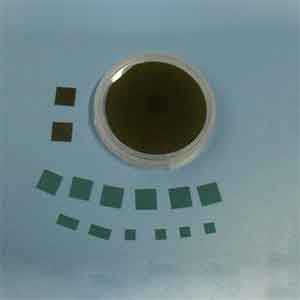
sic wafers in individual containerWe have are a leading SiC wafer supplier with a large selection of SiC wafers at low cost available and in stock. Please send us your specs/qty today!

Buy online and start your research today!

Get Your Quote FAST! Buy Online and Start Researching Today!

Company:

How SiC Wafers Are Made

Unlike the traditional silicon-based CMOS process, the manufacturing of SiC wafers is a batch process. Once a boule of SiC crystal is grown into individual wafers, they are loaded into a batch lapping system. The system reduces the thickness and makes the top and bottom surfaces parallel. Then, each wafer is manually unloaded, measured, and sorted according to thickness.

The preparation process is vital to the fabrication of a high-quality SiC wafer. To achieve the desired level of surface hardness, the oxidation of the silicon wafer is performed. In addition, the density of dislocations and scratches must be kept below a certain level. If the surface is too rough, a wire saw is used to roughen it. While this is a labor-intensive and expensive process, a high-quality SiC wafer will be the result of this careful preparation.

X-Trinsic offers a wafer reclaim process. This process removes the damaged surface layer from the wafer and repolishes it to restore it to device-ready state. This process can save a company a great deal of money, since it does not require the purchase of a new wafer. Also, this method can increase the yield of a given wafer by as much as 50%.

Current production of SiC wafers is done using a batch tool. This method has a low throughput, so it is limited to smaller wafers. However, as production of larger-size wafers continues to grow, the batch tool's throughput will decrease. It will be unable to handle 12 150 mm and nine 200 mm, as of now. Because of this, the industry will have to adapt to the new process.

The production of SiC wafers is an intricate process. It involves the use of a reclaim process. It removes the damaged surface layer from a wafer. It is then repolished to a device-ready surface. Because of its high cost, reclaims are not an ideal choice for final solutions. Aside from the reclaim technique, another method is the wafer reclaim.

The process of making SiC wafers involves the lapping of a silicon substrate with a wire-saw. A specialized wire-saw is used in the process, but the wire-saw may be too expensive. It may also be prone to damage to the subsurface. In this case, a Pureon suspension is an ideal solution for the entire process. Further, it is a highly economical and flexible solution for processing SiC wafers.

In order to produce silicon wafers, the silicon crystals must be grown in reaction cells with an interior volume between six and twelve times the volume of the crystal. Afterwards, these crystals are cut into individual chips. The final wafers are then chamfered to make them thin enough for reflowing. As a result, the silicon-based chips are much thinner than conventional semiconductors.

In addition to manufacturing, the SiC industry is moving to larger wafer sizes. As the size of silicon wafers increases, batch processing loses its advantages. Currently, a batch tool can only accommodate twelve 150 mm or nine 200 mm silicon wafers. By contrast, two 200 mm batch tools can accommodate up to nine wafers each. This process is a time-consuming and expensive method, but it's the future of semiconductors.

During the manufacturing process, the silicon carbide crystals are checked for their dislocations. This is done by evaluating the area of the wafer and assessing the shape of the crystal. A defect can affect the overall performance of a semiconductor. Once a defect is discovered, it is removed by the company. During the manufacturing process, silicon carbide wafers are sliced into individual chips.

After a silicon substrate is manufactured, it is processed to ensure that it has the highest purity possible. In addition, the process can create defects in the epitaxial film if it is not processed properly. The resulting wafers are not only better-quality but also more efficient. They can be made to match the requirements.

Video: Fabricating SiC Wafers

Companies That Manufacture Silicon Carbide (SiC)

There are several companies that manufacture silicon carbide (SiC) products. Some of the leading companies in the field include:

  1. Cree Inc.
  2. Rohm Semiconductor
  3. GeneSiC Semiconductor Inc.
  4. Infineon Technologies AG
  5. STMicroelectronics
  6. Toshiba Electronic Devices & Storage Corporation
  7. Nippon Steel Corporation
  8. United Silicon Carbide, Inc.
  9. Jiangsu Changjing Xingyao High-tech Ceramics Co., Ltd
  10. Littelfuse, Inc.

These companies offer a range of SiC-based products, including power devices, sensing and control, and high-temperature materials.


What Is a SiC Wafer?

SiC wafers are semiconductors made from silicon carbide. Developed in 1893, this material is ideal for a variety of applications. In particular, it is excellent for Schottky diodes, Junction Barrier Schottky diodes, switches, and metal oxide semiconductor field-effect transistors. Because of its high hardness, it is a great choice for power electronic components.

Today, the semiconductor industry is expanding at a rapid rate, which means that wafer supply is crucial to success. To accommodate the increased demand for SiC semiconductors, chipmakers are increasingly turning to both in-house and external sources to create the necessary silicon and SiC wafers. These in-house sources will help chipmakers realize economies of scale and reduce costs. What is a typical silicon carbide wafer?

Currently, there are two main types of SiC wafers. The first type is the polished wafer, which is a single silicon carbide disc. It is made of high-purity SiC crystals, and can be 100mm or 150mm in diameter. It is used in high-power electronics. The second type is the epitaxial crystalline silicon carbide wafer. This type of wafer is created by adding layers of single silicon carbide crystals to a surface. This method requires precise control of the thickness of the material, and is referred to as n-type epitaxy.

The next type is beta silicon carbide. Beta SiC is produced at temperatures higher than 1700 degrees Celsius. Alpha carbide is the most common, and has a hexagonal crystal structure similar to Wurtzite. The beta form is similar to diamond, and is used in a few applications. It has been the preferred choice in power semis for electric vehicles. Several third-party SiC wafer suppliers are currently working on this new material.

A SiC wafer is a semiconductor material made of silicon. A silicon carbide wafer is a crystalline material that is made by etching the crystal. It is typically thin enough to be used for power semiconductor devices. The other type is a type of insulator. The temperature range is extremely important for electrical and magnetic fields in power semiconductors. A silicon carbide wafer is conductive in both directions.

A SiC wafer is a semiconductor material that has excellent electrical and thermal properties. It is a high-performance semiconductor that is ideal for a wide variety of applications. In addition to its high thermal resistance, it also features a very high level of hardness. Compared to other semiconductors, a silicon carbide wafer is ideal for a wide range of power and voltage applications. This means that it is suitable for a variety of electrical and optical devices.

An MSE SiC wafer is the most popular semiconductor material available. It is a high-quality semiconductor material that is perfect for many applications. The MSE silicon carbide wafer is a very useful material for various kinds of electronic devices. MSE supplies offers an assortment of high-quality SiC wafers and substrates. These are available in both n-type and semi-insulating forms.

A SiC wafer is a semiconductor made of silicon. Its flatness, thermal conductivity, and electrical conductivity make it an ideal carrier for silicon. While the 150mm diameter is still the standard, there are several companies that produce 200mm-diameter SiC. A SIC wafer can be produced in a number of different ways, but the most common size is the one used for power conversion.

The 200-mm wafers can be used for a variety of applications. These wafers are 50% thinner than the standard silicon wafer, so the 200-mm diameter can be used for more SiC devices. The 200-mm size is much more efficient and will allow more devices to be built on the same size. A 200-mm-diameter SiC is a very expensive semiconductor, but its high yield makes up for this disadvantage.

In addition to its cost, SiC devices require modules, packaging, and a large amount of silicon. However, the cost of these components has yet to fall sufficiently. These manufacturers, however, need to know the exact specifications of the modules they are planning to use in their products. These requirements are often set by a manufacturer's ASP. The ASP is the maximum price at which they can achieve their goals.

 

What is a Schottky diode?

Advantages of Silicon Carbide Schottky Diodes:

There are many benefits of silicon carbide Schottky diode over other types of semiconductors. For one, they have a low forward voltage drop and high switching speeds. They have excellent performance and are suitable for power systems and electric vehicle charging stations. These semiconductors are AEC-Q101 qualified and available in 650-V and 1200-V versions. Here are some of the most important features of silicon carbide Schottky diordes.

One of the advantages of silicon carbide Schottky diode is its superior switching performance, high efficiency, and power density. They also have a low forward voltage drop and are less prone to thermal runaway. Because they are highly efficient and have a high forward voltage capability, they are suitable for use in power electronics. They are available in various sizes and can be used to build a wide range of electrical devices.

Another advantage of silicon carbide Schottky diode is its low forward voltage drop. Unlike conventional semiconductor devices, the MPS diode wastes very little energy as heat. Consequently, it is ideal for photovoltaic applications. In grid-connected systems, they are used to prevent batteries from being discharged by the solar panel at night. They also prevent reverse current from flowing through shaded strings.

Despite its low forward voltage and low reverse leakage current, silicon carbide Schottky diode offers higher efficiency, power density, and low system costs. Its advantages are its high forward voltage, zero reverse recovery, and good thermal stability. The downside is that the reverse leakage current is higher than the forward voltage, which makes it a poor choice for most applications. So, when choosing a silicon carbide Schottky diod, choose a silicon-metal device.

As a general rule, silicon carbide Schottky diode performance has improved in recent years. They are more efficient than silicon-based diodes. They have low forward voltage and a large band-gap. Its reverse leakage current is less than half that of standard diodes. The high forward voltage of these diodes is also better than those of the standard diodes.

Silicon carbide Schottky diodes have low forward voltage and high reverse-recovery properties. They are a good choice for power-efficient photovoltaic systems. Unlike conventional solar panels, their high forward voltage is low. Because of their low resistance, they are ideal for use in power supplies. They can be used in a wide range of applications and are designed to be compatible with a wide variety of devices.

The benefits of silicon carbide Schottky diode over other semiconductors include lower systems cost and better efficiency. They are a good choice for power-hungry applications, as they offer high efficiency, low forward voltage drop, and fast recovery. The benefits of these semiconductors are many. They are ideal for energy-efficient solar powered systems. This material has a low forward voltage and is able to withstand high temperatures.

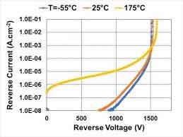
A silicon carbide Schottky diode is used as an alternative to conventional silicon-based semiconductors. Its P-N junction is characterized by a wide band-gap. The silicon carbide Schottky dioide has low forward voltage. Its reverse-biased state inhibits the flow of electric current. Moreover, the SiC Schottky diode's reverse-bias characteristic is independent of the device junction temperature.

The advantages of silicon carbide Schottky diode over conventional silicon-based semiconductors are its power density and efficiency, and their low forward voltage. The low forward voltage and high reverse bias can make it an attractive choice for many applications. The high forward voltage and low forward voltage also make it ideal for power-hungry electronic applications. Aside from their high efficiency and power-hungry features, these semiconductors are also extremely efficient, and their price is not bad at all.

In addition to their high efficiency, silicon carbide Schottky diode has low reverse voltage. In other words, it can handle higher voltages and operating temperature. A typical SiC semiconductor can withstand 50V of reverse voltage before it begins to breakdown. The disadvantages of SiC diodes include high-temperature resistance and a high reverse current limit. The other major difference between the two types of semiconductors is their reverse-voltage behavior.


Video: Silicon Carbide Schottky Diodes Explained

What is Silicon Carbide Junction Barrier Schottky Diodes?

Among the benefits of the JBS device is its high blocking voltage and fast switching rate. It is also characterized by lower forward voltage drop and lack of a depletion layer. However, this material does not store charges and therefore, it is not used in high-voltage applications. Moreover, it does not have an intrinsic p-type semiconductor. It is an excellent choice for n-channel transistors and other electronic devices.

The characteristics of JBS diodes depend on several parameters. The ideality factor, which is the sic wafer junction barrier schottky diodesheight of Schottky barrier, is related to the forward current density in the VF. The drift region resistance, Ron, is the same as the one in the channel. This information has already been presented in Equation 1. The depletion width is approximately 0.8 um perpendicular to the c-axis, which is a good value for analytical calculations.
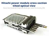
Another important characteristic of JBS diodes is that they are very difficult to corrode, and they are not susceptible to corrosion. Moreover, these semiconductors can withstand high-voltage levels. The high breakdown voltage makes them a suitable choice for space-based electronics. Its wide bandgap characteristics also make it a viable material for use in many applications, from space travel to medical equipment.

The second feature of JBS diodes is their ability to reduce the surface concentration of the insulating barrier grid. This property is important for semiconductors. The resulting junction voltage is high enough to ensure high-quality semiconductors. The third characteristic of SiC JBS diodes is their high switching speed and low noise. They are ideal for power systems and electric vehicle charging stations.

A JBS diode is a type of junction barrier semiconductor with a high Schottky barrier. A junction barrier is a barrier formed between two semiconductors with opposite polarity. This barrier allows a conventional current to flow from one side of the diode to the other. Hence, the JBS diode is a great choice for space-related electronics.

The JBS diode was a great improvement over the PiN diode in a number of ways. The JBS diodes had high forward voltage and high blocking voltage. They had low reverse recovery current and had lower on-resistance. The advantages of this type of junction barrier over the PiN diode are that they are used in different types of electronics.

The JBS diode has a relatively low reverse voltage, due to its high reverse leakage current. Its reverse voltage is comparatively low, so it is a great choice for power converters. Because of its higher doping content, these diodes also have a high forward voltage. They are also very robust, but they are limited to a small area.

The JBS diode has similar forward voltages as the PiN diode. However, the JBS diode has a higher on-resistance and reduced leakage current. This makes it a good choice for power systems and electric vehicle charging stations. These devices are AEC-Q101 qualified and are available in various voltages and current ratings. If you're looking for a high-quality JBS diode, we recommend checking out ROHM Semiconductor.

A JBS diode is a good choice for power devices. They have similar forward voltages to the PiN diode, but the JBS diode's on-resistance is higher. This combination of high on-resistance and low reverse leakage current makes it an excellent choice for power applications. This characteristic makes it a suitable choice for a variety of different applications.

Compared to the PN diode, a SiC Schottky barrier diode has a low forward voltage. It has a high reverse voltage. The silicon and PN diodes have similar characteristics. The main difference between them is the reverse voltage. The former is lower than the latter, while the latter is more expensive. Its forward voltage and its sensitivity also make the JBS a better option for switching mode power supplies.


Video: Silicon Carbide Junction Barrier

What Are Silicon Carbide Switches Used For in Power Electronics?

Silicon carbide (SiC) is a material that has many properties that are useful for power electronics. It sic switch examplehas a larger bandgap than silicon, and has a greater dielectric breakdown strength than either silicon or germanium. Hence, it is ideally suited for power electronics applications. Its low specific on-resistance and high blocking voltage help it support high voltages for shorter distances through a device. This helps it achieve low power losses and reduced electrical resistance.
Silicon carbide switches are highly efficient, high-voltage semiconductors. They can handle higher voltages and frequencies without compromising their performance. They can be made smaller and lighter than conventional silicon devices. They also have high thermal conductivity. They are particularly suited for power applications, where they are needed to minimize switching losses. They also have a long life span and are very durable. For example, a 650-V SiC MOSFET from Toshiba offers low ON-resistance and fast switching.

Because of their low ON-resistance and high bandgap, silicon carbide is ideal for power applications. They offer higher efficiency, smaller size, and lower power consumption. These characteristics also help reduce the overall system size. They can withstand voltages up to 3,000V. In addition to power applications, they are ideal for solar inverters. Besides power electronics, they can be used in industrial machinery.

Another benefit of using silicon carbide is that they are more durable. Its high thermal conductivity and low ON-resistance makes them more suitable for power applications. The result is that these switches can withstand high temperatures and provide increased reliability. These benefits make it an excellent choice for power electronics. Its high temperature resistance, low ON-resistance, and low on-resistance make them ideal for a variety of uses.

While silicon carbide is a popular material for electrical and optical applications, the benefits of silicon carbide switches are primarily attributed to their higher voltage and frequency capabilities. In addition to being durable, these switches are lightweight and offer low thermal resistance. The combination of both materials has advantages over conventional silicon. Its high operating temperature ranges and low inductance reduce switching losses and improves system efficiency. This is one reason why this material is so popular in power electronics.

Silicon carbide is more expensive than silicon, but has many advantages over traditional materials. The material's higher electrical conductivity and lower on-resistance allow for higher power density. Furthermore, its low ON-resistance and low total gate charge allow for fast switching and reduced power consumption. These features are critical to improving the performance of power electronics, which are increasingly sensitive to thermal stress. With these properties, silicone carbide can be used in a variety of different applications.

Silicon carbide is a form of carbon and silicon. It is an electrical insulator in its pure form. However, it can be made into a semiconductor by introducing impurities. Doping silicon carbide with aluminum, boron, and nitrogen will yield a P-type material, and a N-type will produce a N-type material. This means that these switches are highly reliable and are a much more flexible material.

Other benefits of silicon carbide power modules include higher voltage, lower switching losses, and improved thermal management. They are highly flexible and can operate at very high frequencies. They can be used in high-speed switching and can be incorporated into various types of devices. A common example is a bulletproof vest. These components can be molded into a variety of shapes. They are used in many applications that require a small size.

Other benefits of silicon carbide are its high bandgap, lower ON-resistance, and high thermal conductivity. These properties allow for a lower-cost, higher-performance product. In addition, silicon carbide is capable of operating at a higher bandgap than its counterpart, making it more efficient in high-powered applications. A large bandgap will allow for better performance in a wide range of applications.

A major benefit of silicon carbide power switch is its low on-resistance and high on-voltage. They also have a higher withstand voltage and have an increased switching frequency. Because of this, they have several advantages in power converter applications. These features allow for greater efficiency and lower cost. They are also smaller and lighter than conventional devices. There are a number of companies that offer these devices. The best ones are reputable and have a good reputation.


Video: Silicon Carbide Switches

Silicon Carbide For Metal Oxide Semiconductor Field-Effect Transistors

The silicon carbide for metal oxide semiconductor field- effect transistor is a transistor that has a gate electrode, a gate oxide layer, and a passivation protective layer. This material is deposited by etching. The semiconductor is composed of a plurality of first conduction type regions. This layer is positioned on a portion of the surface of the first SiC contact layer.

These devices have several advantages over conventional silicon-based devices. Their low parasitic resistance makes them particularly suitable for microwave power conditioning applications. Their high thermal conductivity, low mobility loss, and high critical breakdown fields make them an excellent choice for these applications. However, they do have a higher price tag than their silicon-based counterparts. It's important to know which material is right for your application before choosing a semiconductor material.

Silicon carbide for metal oxide semiconductor field-effect-transistors (MOSFETs) are an excellent choice for applications that require high-speed switching. These devices have superior performance in microwave power and low-frequency power conditioning. They also have high thermal conductivity, making them suitable for microwave and low-frequency power conditioning applications. These transistors are now in mass production. If you're interested in finding out more about this new material, take a look at this article!

A good example of a silicon carbide MOSFET is the Wolfspeed Silicon Carbide MOSFET. These devices offer excellent performance in switching applications. Compared to their silicon counterparts, they feature improved critical breakdown strength, lower switching losses, and greater operational temperatures. Moreover, silicon carbide MOSFETs are more compact, reliable, and lightweight. These properties make them ideal for use in mobile phones and portable computers.

Silicon carbide MOSFETs have many potential benefits. Its increased efficiency, higher switching frequency, and lower switching temperature make it a superior semiconductor for power conversion. As a result, it has become the most popular semiconductor material for MOSFETs. They are now being produced in large quantities in the form of CMOS and NCMOS. So, the silicon carbide MOSFETs are a good choice in a wide range of applications.

The Silicon carbide MOSFET is a common semiconductor for power transistors. Its advantages include high thermal conductivity and low parasitic resistance. Its benefits are beneficial in both microwave and low frequency power conditioning applications. These devices also have a low EMI/RFI filter. The silicon carbide MOSFETs can be used for a variety of applications. The most popular MOSFETs are a great way to save money while powering your home.

One of the best features of silicon carbide MOSFETs is their low thermal conductivity and low parasitic resistance. This material is suitable for power applications in microwave and low frequencies. In addition, it also has low thermal resistance. These characteristics make SiC MOSFETs an excellent choice for many applications. Its intrinsic advantages make them superior for use in high-power, microwave, and ultra-low frequency power conditioning.

The silicon carbide MOSFETs are used in power amplifiers and switching applications. They are used in electric vehicles for control systems and in renewable energy sources. They are used in audio-frequency power amplifiers. As with all semiconductors, silicon carbide is the dominant material in MOSFETs. It is much more efficient than silicon and can handle higher currents and voltages at the same thickness.

A silicon carbide MOSFET is a device that is made from silicon and a silicon oxide semiconductor. The materials are different in structure and can affect the characteristics of a MOSFET. In general, silicon carbide is the dominant semiconductor in MOSFETs. This material is less efficient than the other materials in semiconductor devices. Unlike the silicon MOSFET, it can be cooled quickly.

The silicon carbide MOSFETs described in this patent have a silicon carbide channel layer and a silicon oxide semiconductor channel. These two materials are compatible and can be used in the fabrication of transistors. A semiconductor cell made of silicon carbide is a circuit that has a low parasitic resistance. The UTB is an inexpensive way to fabricate a silicon carbide MOSFET.

What is 4H Silicon Carbide (SiC)?

If you're not sure what 4H-SiC is, it is a semiconductor with a low bandgap density and is ideal for power electronic applications. Its defect density is similar to that of silicon, but its crystalline structure is very different. It has a higher dislocation density than silicon, and requires a single fabrication platform to be produced. Its low-k structure makes it ideal for sensors and high-temperature circuit evolution.

silicon carbide wafers 4h vs 6h performaceThe cubic unit cell polytype of silicon carbide is 3C-SiC, while hexagonal units are 6H-SiC or 15R-SiC. In order to achieve periodicity, atomic layers with cubic symmetry alternate with those of hexagonal symmetry in a regular pattern. The most common polytype of four-dimensional SiC is 2H-SiC, while the cubic unit cell is the most abundant type.

The material's electrical properties are also quite superior to those of SiO2, and its low-field mobility and high avalanche breakdown electric field are among the most attractive properties. In order to develop these devices, device simulation technology is necessary. In fact, this technology builds on the pioneering work of Ruff, and is often used to design SiC power devices. As a result, much effort has gone into improving this technology.

The FTIR spectra of as-grown 4H-SiC were recorded in transmission mode at room temperature. The FTIR data of the molecule can be seen in Figure 4. A prominent peak at 790 cm-1 is associated with Si-C bond excitation and vibration. This peak is responsible for the characteristic of tetrahedral structure. Its crystallization is a result of the formation of dangling bonds in the amorphous structure.


For the most part, we know that four-helix silicon crystals have a relatively large bandgap. This is a 4h silicon carbide waferscharacteristic that is very important in power electronics. In addition to its optical properties, four-helix silicon has incredible structural, optical, and electrical properties. It is also incredibly hard to work with due to its high process temperature and chemical stability. SiC is composed of over 200 polymorphs, but only four are of interest to power electronics.
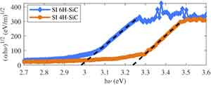
Four-helix silicon (CHSiC) is a semiconductor that has a high defect density, compared to crystalline silicon. The symmetry of four-helix silicon is hexagonal, while the symmetry is cubic. Because the atoms in four-helix silicon are hexagonal, they are oriented into only three possible positions. However, this symmetrical feature is not sufficient to form a four-helix silicon crystal. To make this material, it must have a symmetrical structure, so it must be a bilayer.

One of the reasons four-helix silicon crystals are useful for electronics is their high breakdown electric fields. A single-helix silicon crystal with a cubic-helix symmetry will tend to produce a 4H-SiC component. A six-helix silicon crystal will contain one-eighth hexagonal and one-half cubic-hexagonal bonds. If you're wondering how four-helix silicon crystals work, the answer is polyhedral, and it's the simplest and most common way to make a four-helix semiconductor.


Video: What is 4H Silicon Carbide?

What is 6H SiC?

6h silicon carbide wafersThere are two polytypes of silicon dioxide: 4H-SiC and 6H-SiC. Four has equal proportions of hexagonal and cubic bonds, while six has two-thirds cubic bonds and one-third hexagonal bonds. In general, they have hexagonal overall symmetry. Each of these polytypes is different from each other, but the unit cell extensions are the same. Hence, we cannot distinguish between the two types of silicon dioxide.
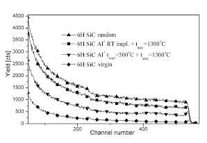
While 3C and 6C SiC are polycrystalline, 6H and 7H are tetrahedral, respectively. They have a cubic structure. Both are essentially similar to zincblende. The only differences are in their structures. The cubic structure is known as a-SiC, while the hexagonal structure is called b-SiC. Its tetrahedral shape allows it to withstand higher pressures than its cubic counterpart.

The growth rate of 3C SiC is several hundred GPa, followed by a 20% volume reduction. Then, the growth rate of 6H SiC is a mere one mm/h. The kinetic and thermodynamic effects are not immediately evident. However, in PVT growth, the polytype occurrence is temperature-dependent. Gas phase stoichiometry plays a critical role in the growth of SiC crystals, and higher C/Si ratios favor the formation of the 4H polytype. Increased hexagonality is linked to higher C/Si ratios.

In addition to 6H and 7H, SiC has the following three polytypes: 2C-SiC, 3C-SiC, and 4H-SiC. The four H polytype is the most stable and the cubic type has the least energy. Similarly, the two wurtzite polytypes are the most stable. All three polytypes have a common carbon (C) atom in the center of the mass.

Compared to zincblende, moissanite-6H SiC (B6) is a cubic tetrahedral crystal structure. The cubicdefinition of 6h silicon carbide wafer structure is the most stable and has the lowest energy. Other types of 6H-SiC are the same, but differ in their atomic arrangements, which makes them a good choice for making crystalline semiconductors. There are several physical properties that distinguish them from one another.

Commercial SiC is a mixture of wurtzite and zinc-blende chemistry. It has two distinct symmetry types, the cubic and hexagonal symmetry. Some of the polymorphs are mixed with a mix of wurtzite and zinc oxide. In addition, 6H-SiC is composed of two-thirds cubic and one-third hexagonal bonds. Other common SiC crystals are 2H-SiC, 15R-SiC, and 15R-SiC.

The most common polytype of silicon carbide is 6H. Other types of SiC are called 15R-SiC, which contains three-fifths hexagonal bonds and two-thirds cubic bonds. SixH-SiC, the most studied, is composed of a combination of wurtzite and zinc-blende crystalline structures. Its hexagonal structure is a blend of wurtzite and zinc.

When the two types of 6H-SiC occur together, they have a different atomic arrangement. While the fourH polytype is a dike, the 15R-SiC is a hexahedral-type. In comparison, the 3C polytype is monoclinic and metastable. When the two are combined, they form a hexagonal-like structure.


What's the Difference Between 4h and 6h Silicon Carbide?

What's the difference between 4h and 6h silicon carbides? The answer depends on the application. The power electronics industry is more interested in polytype 6H because it is easier to grow. The difference between polytypes is determined by dislocation density, which affects the quality of the crystal. The differences between polytypes include stacking faults, carbon inclusions, and big voids.

While a high-voltage application might call for a higher breakdown voltage, silicon carbide is more efficient. This translates into higher yields and less production cost. This material switches at a rate nearly ten times faster than silicon, allowing high-power devices to be made with smaller wafers. Also, because of its higher resistance, it can withstand ten times more electrical fields.

Another significant difference between silicon carbide and other semiconductors is the bandgap. The difference between the two is based on how each crystallizes. Silicon is a solid with a narrow bandgap. The bandgap is the distance between the atomic layers of a material. A narrow bandgap makes it difficult for electrons to move to the conduction zone. In addition, the gap is also more dense, which means that it is more difficult to transfer energy from one layer to another.

The biggest difference between the two types of silicon carbide is the breakdown voltage. Silicon is 1 to 1.5 eV while silicon's bandgap is between 2.3.3 eV. In terms of electrical properties, silicon carbide is much more dense than its counterpart and offers better EMI and EMC compatibility. However, it has a higher capital expense. This is due to the fact that its manufacturing process is limited to six-inch-wide wafers, while the silicon is unable to handle this size.

When comparing silicon carbide, 4H is the more expensive of the two. It is more expensive, while 6H is more efficient and compact. The four-hour version is easier to manufacture, and the 6h version is more durable. In addition, it is more durable. Compared to the four-hour silicon, the 6-hour silicon carbide is more than twice as dense as the four-hour silicon.

Although 4h is cheaper, silicon carbide is better for high-voltage applications. The higher voltage enables higher-voltage applications. It is also more efficient than its silicon cousin, but it is not as compact. Its larger size also means it is more costly. But the benefits of 6h silicon are more important to the electric vehicle industry. So, what is the difference between 4h and 6h?

In commercial silicon carbide, the four-hour silicon carbide is more dense than the six-hour version. It has a larger bandgap, which means electrons are more difficult to move to the conduction band of silicon. It is also less expensive than 6h. The 4hour silicon is a higher-voltage semiconductor and resists heat more than sixhours of electricity. So, it's not surprising that the lower-voltage version is the best.

The main difference between 4h and 6h silicon carbides is the bandgap. While the four-hour silicon carbide has a higher bandgap than its hexagonal counterpart, it is also less expensive to manufacture. In this case, 6h silicon carbide is more durable, while 4h is better for high-voltage applications. The six-hour variant has higher resistivity.

Aside from its higher cost, the 4h silicon carbide is cheaper to manufacture. The difference between the four-hour and six-hour silicon carbide is mainly in the shape. The smaller size of the four-hour silicon carbide compared to the six-hour version can help the company make more money. In addition, silicon carbide is more expensive to produce than the four-hour silicon.

The difference between 4h silicon carbide and 6h silicon carbide is a little confusing. They are similar in structure, but their chemistry is different. The 2h silicon carbide is the most common form of silicon, while the cubic one is the most expensive. In contrast, the 6h silicon carbide is twice as expensive and is harder to fabricate. It is an excellent choice for electrical applications, but you should check the specs and the price before you purchase it.