Silicon-on-Insulator (SOI) Wafer - An In-Depth Study
What is SOI?
Silicon on Insulator (SOI) is a manufacturing method that reduces the capacity of parasitic components and thus increases performance. Si wafers are the main components of the integrated circuits found in our daily electronic devices. SI wafers are the main component of an integrated circuit found on a wide range of devices including smartphones, tablets, computers and other electronic devices.
Si wafers produced in this way are suitable for the production of mobile phones, and to give you an overview, here are the different production methods for SOI.
Get Your Quote FAST!
SOI Wafer Bonding Descriptions
In wafer bonding, the surface of the two wafers is covered with an oxidising layer and the oxide layer is bonded to the surface of the silicon.
The insulating layer holds the two wafers together, while the oxide layer is buried under the semiconductor stage (BOX). Once the desired thickness of semiconductors is reached, the surface of the wafer is polished and overlapped.
SIMOX SOI
The process creates a layer of buried oxide resin by irradiating a semiconductor wafer with oxygen ions and curing it at high temperatures. The ion energy determines the thickness of the intrinsic semiconductors, and the amount of oxides in the resin increases with the energy of the ion.
SMART CUT SOI
In this method, hydrogen ions are used to control the thickness of the top silicon layer, while after the implantation process, hydrogen ions are repelled in a size-controlled manner. This gap can be reused to produce other SOI wafers, and this method can also be used for other purposes, such as the production of new silicon chips.
An in-depth study on Silicon on Insulator (SOI) Wafer
Introduction.
The fabrication of micro-electromechanical systems (MEMS) or complementary metal-oxide-semiconductor 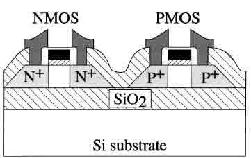 (CMOS) based integrated circuits have a common requirement of silicon on insulator wafer material as the main material. Silicon on insulator-based wafers are widely used as they require low power compared to other wafers when manufacturing them and also one can produce high-speed devices. The mechanical characteristics of mono-crystalline films are better than the polycrystalline silicon counterparts making it favorable for use in MEMS applications. The wafers are made of three layers i.e. the device layer (primary quality silicon layer), a buried oxide layer (an electrically insulating layer made of silicon dioxide providing vertical isolation from the substrate), and the handle layer. Besides, monolithic semiconductor circuits that use a dielectric rather than junction isolation are preferred and this is achievable when silicon on insulator wafers are used (G. K. Cellera, 2003).
Figure 1: A schematic architecture of a silicon on insulator (G. K. Cellera, 2003)
The discovery that silicon on insulator (SOI) circuits had the needed radiation harness that occurred between the 1970s and the 1980s spearheaded the acceptance of SOI substrates. The thin active silicon layer did reduce the effects of ionizing radiation on the performance of the device by ceasing the movement of majority charges that are generated by alpha particles affecting the silicon substrate.
Silicon on Insulator Fabrication Process
Three methods can be used to make silicon on insulator-based wafers. The methods used to determine the substrate that is to be obtained. A method is selected based on the intended user application.
1. Bonded and Etchback Silicon on Insulator (BESOI) approach
This method was introduced by Latsky and it is based on introducing an etch stop (oxide layer) before bonding 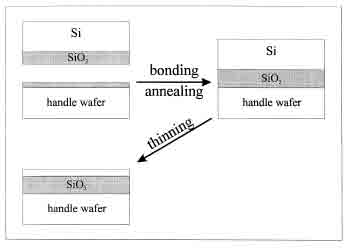 a wafer pair. The bonding process is done at different temperature ranges and the result is a buried oxide layer on the wafer. The wafer is then etched till a thin silicon layer is left. The formed layer is known as the device layer while the other layers make the handling substrate. This method is advantageous as it results in the formation of a crystal layer that is perfectly crystalline. However, the silicon layer formed does have a nonuniform thickness as a result of the etching process (Mozumeder, 1996).
One wafer is oxidized to reduce the defects at the interface existing between silicon and silicon dioxide with an existing silicon oxide covered wafer. An annealing process is done to the oxidized wafer followed by a thinning process that has to be mechanically done. With the current technology, it is possible to thin the device layer to less than 100nano meters with a variation allowance of 10 nanometers. Testing of etch stops has to be carried out consistently to improve the device layer uniformity thickness. The etch stops also do protect the device layer to the point where the sacrificial layer has been eliminated. This method is currently being used to make thick layer SOI substrates that require simple grinding and polishing operations.
2. Separation by Implantation of Oxygen (SIMOX) approach
In this semiconductor fabrication method, oxygen is implanted into the silicon layer in significant proportions. 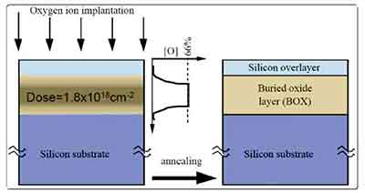 Introducing oxygen ions beneath the surface of a silicon wafer results in the formation of a buried layer of silicon (iv) oxide. The amount of energy possessed by the oxygen ions defines the range and profile of the implanted layer. The inherent implant damages have to be removed by high-temperature annealing. Annealing also contributes significantly to the redistribution of oxygen atoms (Jean-Luc Leray, 1996). This leads to the formation of a buried oxide layer. The ion energy plus the effect of oxygen aid in determining the thickness of the buried oxide layer and top silicon layer of SOI wafers formed by this method has a good uniformity plus the defect density is low. With this method, thin-film silicon on insulator wafers can be produced on a large scale (Asadollahi, 2017).
3. Smart Cut Approach
In the case where silicon on insulator wafers with extremely top thin silicon layers that have a thickness of fewer than 1.5 micrometers are needed, the smart cut approach has to be used. This is because this method produces high-quality SOI substrates by combining direct wafer bonding and layer transfer by ion implantation (I. Radu, 2008). By using this method, we have flexibility on the top layer silicon thickness as the transfer film has a direct relation to the implantation energy.
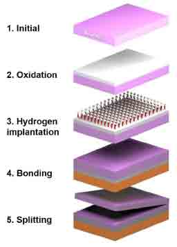
Figure 4: An illustration of the smart cut method. (Seung Min Lee, 2017)
Advantages and disadvantages of Silicon on Insulator Wafer
Silicon on insulator-based wafers when used makes it possible to produce devices that are relatively fast 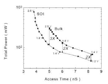 compared to bulk silicon devices while operated at the same voltage and using similar digital logic circuit principles. Besides, SOI-based wafers can be used at operating voltages they are lower than the other wafers thus contributing significantly to a lower power consumption rate (G. K. Cellera, 2003). In this wafers, active devices are vertically and laterally isolated from the substrate excellently. The inter-device leakage or latch-up that exists in CMOS structures is eliminated while using this wafer. Additionally, high-quality inductors can be fabricated since substrate coupling is minimized in radio frequency circuits. Lastly, devices having mixed-signal integrated circuits have reduced interference.
Figure 5: An illustration of the execution time behavior while using SOI. (Rahul Kr. Singh, 2011)
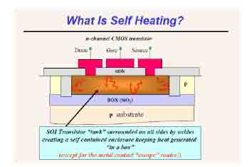 When using this technology, one has to consider the costing of the substrate as it is generally high. Besides, the complexity of fabricating the substrate material introduces overheating issues in the devices made using this wafer. In addition, silicon oxide has a low thermal conductivity characteristic thus limiting its use (Seung Min Lee, 2017). Research is currently been undertaken and there are results indicating that the inherent limitations while using this wafer can be minimized.
Applications.
Silicon on insulator-based devices are applied in high-performance radio frequency circuits or in minimizing the short channel impacts experienced in microelectronic gadgets. These wafers can be used to make microprocessors and high-performance memory units such as SRAM.
Conclusion.
Given the fact that we are technologically nearing our end of the read situation, silicon on insulator technology is a technique that is to allow the traditional use of silicon material in today’s devices as we buy time for the discovery of better materials to be used in the next few years.
Silicon on Insulator Application References
Andreas PloÈ ûla, G. K. (2000). Silicon-on-insulator: materials aspects and applications. Solid-State Electronics, 775-782.
Asadollahi, A. (2017). Fabrication of Group IV Semiconductors on Insulator for Monolithic 3D Integration. Stockholm, Sweden: KTH Royal Institute of Technology.
G. K. Cellera, S. C. (2003). Frontiers of silicon-on-insulator. JOURNAL OF APPLIED PHYSICS, 1-25.
I. Radu, A. B. (2008). Fundamentals of Wafer Bonding for SOI: From Physical Mechanisms Towards Advanced Modeling. The Electrochemical Society, 349-360.
Jean-Luc Leray, P. P.-L. (1996). An Overview of Buried Oxides on Silicon: New Processes and Radiation Effects. Journal de Physique III, 1692-1646.
Mozumeder, B. (1996). Development of Bonding and Etchback Silicon an Insulator Wafers. 14th Annual Microelectronics Engineering Conf (pp. 30-33). Rochester Institute of Technology.
Rahul Kr. Singh, A. S. (2011). SILICON ON INSULATOR TECHNOLOGY REVIEW. International Journal of Engineering Sciences & Emerging Technologies, 1-16.
Seung Min Lee, J. H. (2017). Advanced Silicon-on-Insulator: Crystalline Silicon on Atomic Layer Deposited Beryllium Oxide. Scientific Reports, 1-7.
