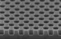
Microwells to Create Free-Standing 2D Materials
An assistant professor requested the following quote:
I am wondering if the University Wafer is selling or producing silicon  wafers with microwell arrays. We need silicon wafer pieces with spherical wells which have ~ 1 um diameter. Our aim is using such wells to create free-standing 2D materials for measuring their mechanical properties.
The well diameter should be around 1 um (could be less than that but not bigger). The depth of the wells could be 100-200 nm as it is not that critical. Depending on how much it will cost I can order 5 wafers. Thank you for your help.
Reference #260344 for specs and quantity.
Get Your Quote FAST! Or, Buy Online and Start Your Research today!
Sapphire Wafers Used to Grow 2D Materials
A doctoral student researching Nanobioelectronics and Biosensors requested a quote for the following:
We are currently in search of sapphire substrates, specifically double-sided polished and fully transparent, for use as substrates in the growth of two-dimensional materials. Ideally, we are looking for substrates with dimensions of 25 x 25 mm and a thickness of 0.5 mm. While browsing your company's sales website, we noticed that the available sizes are mainly 50 mm and 100 mm. We anticipate requiring a quantity of 50 or more substrates. Could you please provide us with a quotation for sapphire substrates of the specified dimensions.
We just use it for experiment. 2D materials grow on the sapphire substrate.
Reference #278810 for specs and pricing.
C-plane (0001) Sapphire Substrate for 2D Material Growth
A PhD candidate requested the following:
Can I ask a question about custom miscut angle sapphire? I need a C-plane (0001) sapphire substrate with miscut angle along A axis (<112-0>) about 0.2 degree as a substrate for 2D materials growth. I was able to find C/M miscut sapphire from several companies (which is usually used for III-V semiconductor growth), but I couldn’t find C/A miscut sapphire in stock. One-side polishing and size equal or larger than 2 inch would be enough. I have attached a relevant paper regarding C/A miscut angle sapphire for 2D material growth. Can you please let me know the price and lead time for this customized sapphire?
Reference #266650 for specs and pricing.
Thermal Oxide on Silicon for 2D Materials Growth
A physics department
instructor requested the following quote:
We would like to order "285nm SiO2 on Si" substrates for our study on the growth of 2D materials.
Could you please give me information about the possible number of
substrates in a packet and their prices?
UniversityWafer, Inc. Quoted
2" P(100) 1-10 ohm-cm SSP 400um with 285nm of Thermal Oxide
2" P(100) 1-10 ohm-cm SSP 500um with 285nm of Thermal Oxide
Reference #185151 for specs and pricing.
Graphene and 2D Materials
A nanotechnology scientist requested the following quote:
I am interested in your commercial graphene wafers.
What I want to do with your graphene wafers is to deposit another 2D materials on it by direct transferring with adhesive tape.
I have some questions:
- Is your graphene conductive enough as bottom electrode?
- s the adhesion between graphene and SiO2 strong fairly? During transferring using adhesive tape, graphene should be intact.
UniversityWafer, Inc. Answered:
- Yes, it is!
- The adhesion is strong but no enough to use adhesive tape for the transfer process.
If you need more information, please let me know.
Reference #190580 for specs and pricing.
WS2 and WSe2 2D Materials
A PostDoc requested the following quote:
Please send me a quotation including the following items:
- Bilayer Graphene on SiO2/Si (10 mm x 10 mm)
- Trilayer Graphene on SiO2/Si (10 mm x 10 mm)
- Monolayer Graphene on SiO2/Si (4" Wafer)
If you can provide other 2D materials, e.g. WS2 and WSe2, I am also interested.
Reference #215004 for specs and pricing.
2D Materials to Fabricating Field Effect Transistor (FET)
A PostDoc needed help with the following:
SiO2/Si wafer. The SiO2 thickness is 290nm. The wafer is used for making field effect transistor of 2D materials especially MoS2, WS2 and WSe2. We are concerned about the maximum gate voltage can be achieved.
Reference # for specs and pricing.
2D Materials Exfoliation
A graduate student studying physics requested the following quote:
I am looking for silicon wafers with oxide layers that are 90nm and 260nm. 100mm diameter would be fine and we'd like 2 of each. It is for exfoliation of 2D materials, so I don't believe the doping is critical. Do you have these?
Reference #222012 for specs and pricing.
4 Inch Thermal Oxide Coated Silicon Used for 2D Materials Research
A Ph.D. candidate researching devices requested the following quote:
We would like to buy about 100 pieces of 4-inches wafers intended for researches in 2D materials. The properties are as follows:
100mm P/B <1-0-0> <0.005 ohm-cm>
525±25µm PRIME SILICON WAFER, SSP,
2 SEMI FLAT, WITH 3,000A+/-5%
THERMAL OXIDE ON BOTH SIDES
Or do you have better recommendations?
This is the first time for me to buy silicon wafers, and I am not familiar with the properties. The wafers are intended for researches on exfoliating Si wafers and fabricating devices. I guess you know what kind of wafer we need.
These wafers are bought by two research groups, 50 wafers for each.
Reference #222235 for specs and pricing.
Fabricating Electronic Devices with 2D Materials
An electrical engineerng Ph.D candidate requested the following quote:
It is a pleasure to contact with you. My research work is involving fabrication of electronic devices based on 2D materials such as Graphene, WSe2 and MoS2.
I need to buy wafers from you for my research work, but Im a little confused about the best options for my research work .
I need P++ silicon wafers ( heavily doped like 10^19 cm-3 or higher) with SiO2 layer on top of it. I need SiO2 layer to be in thickness between 50 nm to 300 nm.
I will use the substrate itself as metal-gate and the SiO2 layer as a dielectric layer for FET devices.
In addition, my experiments will be done at high temperatures (like 800-1000 degrees Celsius).
At this stage, the diameters and orientation are not crucial, but we prefer diameters 100 or 150 mm if they are available.
Could you please give me your recommendations for the best options?
Reference #228993 for specs and pricing.
Undoped Silicon for 2D Materials
An Assistant Professor of a Physics Department requested the following quote:
Do you have good-quality undoped silicon wafers? We need to use them as substrates for 2D materials.
UniversityWafer, Inc. Quoted:
Item #2019 - 50.8mm Undoped (100) >10,000 ohm-cm 280um DSP
Reference #272176 for specs and pricing.
Calcium Flouride for Optical 2D Materials
A PhD in materials engineering requested the following quote:
Looking for CaF2 substrates for optical 2D materials measurements. Substrate size around 8x8 mm^2. works is mostly in reflection with AFM and require high surface smoothness (atomically flat) and flat dielectric function between 1-11 micron.
Reference #272952 for specs and pricing.
Quartz Wafers for 2D Material Research
Researchers have used the following fused silica windows for their 2D Material Research.
Fused Silica
Item #2090
150mm Fused Silica JGS2 500um DSP Surface Roughness <1nm
Item #3120
125mm Fused Silica JGS2 300um DSP Surface Roughness <1nm
Single Crystal Quartz Also available.
Single Crystal Quartz
Item #555
100mm ST-cut 500um SSP Angle:42°45' Seeded (WITH-SEED)
HOPG Substrates for Fabricating 2D Materials
A chemical engineering PhD candidate requested a quote for the following:
I'm looking to buy HOPG as a substrate for 2D materials. Could I have a quote for HOPG of size 10*10*0.5mm?
Reference # 255966 for specs and pricing.
What is the Best Silicon Wafer Spec for Growth of Thin 2D Materials?
Choosing the best silicon wafer specifications for the growth of thin 2D materials depends on several factors,  including the specific 2D material you're working with, the intended application, and the growth method used. However, there are some general guidelines that are often followed in the research and fabrication of 2D materials like graphene, transition metal dichalcogenides (TMDs), and others:
-
Orientation: The crystallographic orientation of the silicon wafer, such as (100) or (111), can be important. For instance, (100)-oriented wafers are commonly used for graphene growth.
-
Doping Level: Low-doped or intrinsic silicon wafers are often preferred. High doping levels can interfere with the electronic properties of the 2D materials.
-
Surface Roughness: Smooth surfaces with minimal roughness are typically desired for uniform growth of 2D materials. The wafer surface should be free of scratches and other defects.
-
Oxide Layer: Silicon wafers with a thin layer of silicon dioxide (SiO2) are frequently used, especially for materials like graphene. The SiO2 layer provides an excellent contrast for visualizing the 2D materials under an optical microscope and can also affect the properties of the 2D material.
-
Thickness of Oxide Layer: The thickness of the SiO2 layer can be crucial, especially for optical contrast and electronic applications. A common thickness is around 300 nm, but this can vary based on specific requirements.
-
Purity and Cleanliness: High-purity wafers with minimal contamination are essential to prevent any unintended interactions with the grown 2D material.
-
Size: The size of the wafer depends on the scale of your experiments or production. Standard sizes like 2-inch, 4-inch, or larger wafers are available.
-
Thermal Properties: Depending on the growth technique (like chemical vapor deposition), the wafer should withstand high temperatures without warping or cracking.
-
Compatibility with Growth Method: Ensure that the wafer is compatible with the specific growth method used for your 2D material (e.g., CVD, MBE).
Each 2D material and growth method might have unique requirements, so it's important to consider the specific needs of your project when selecting a silicon wafer. Collaborating with a knowledgeable supplier like University Wafer, Inc., which has expertise in this area, can be very beneficial in selecting the right substrate.
What is 2D Material Research
Although 2D material-based technologies are not yet widely used in commercial applications, these materials have been the subject of considerable research interest in recent years. The newly discovered class of graphene, a material with the potential to enable new electronic and photonic devices, has led to a number of exciting new applications for graphene, but has only recently been discovered. What is it about and what does it mean for the future of electronics, photonics and electronics in general? Like graphene, it requires an immature 2d material, which makes it difficult to report on its properties and potential applications. [Sources: 0, 9, 15, 21]
In 2013, Penn State Materials Research Institute took up this challenge, and since its appointment, research in this area has focused on the discovery of novel 2D materials other than graphene. The focus of experimental research is on the investigation of the properties and properties of graphene and its potential applications in electronics, photonics and other applications. In addition to application-oriented use, a new class of 2D materials for manufacturing and structuring can be developed, which can include a precise matching of their properties for use in a wide range of applications, such as electronic and photonic devices. [Sources: 1, 9, 11, 17]
The largest class of 2D materials are transition metal dichalcogenids (TMDC), a range of materials with polyatomic structure. In this case, the researchers have succeeded in implanting atoms in a stacked 1D material with two different properties. In a study published in the journal Nature Materials, they showed that by changing the way it is exposed to the chemical vapour deposition (CVD) process used to produce this material, the material could yield two types of properties. Single-layer materials, sometimes referred to as "intermediate materials," are crystalline materials consisting of a single layer of atoms. [Sources: 2, 10, 16, 18]
Chilkoor and Gadhamshetty continue their work to build nanocoatings to prevent corrosion in agriculture and other applications. Their calculations serve as a model for a research group at the National University of Singapore, which was able to produce 2D materials in its laboratory. [Sources: 8, 10]
The project is part of a larger effort to understand the interactions between molecules in 2D materials to uncover the mechanisms of Raman amplification in them. This technique comes when we start to see different types of transistors that are made entirely of two-dimensional (2-D) materials that contain graphene, tungsten diselenide, and other materials such as graphene - such as nanocoatings. These newly emerging 2d materials differ from graphene in that they increase the functional diversity of their devices. Research on 2D materials is maturing at the point where we have developed and continue to develop a new class of high-performance and low-cost materials for a wide range of applications. [Sources: 5, 9, 16, 20]
The research team plans to incorporate this new material library into storage devices for practical applications and to intercalculate foreign atoms to use novel functionalized ICs in 2D materials. [Sources: 4]
In Nash's group, we are exploring new materials, including 2D materials such as graphene and metasurfaces. Graphene research focuses on the quantum domain of the NPL, and we focus our research on graphene research. Invited Presentations and Speeches at the Annual Meeting of the American Chemical Society in Washington, D.C. [Sources: 11, 13, 22]
This puts us in a unique position to respond to the needs of industry, to create the materials that are needed next, and to develop the technologies to produce them. [Sources: 6]
Research in the Nanostructured Materials group includes the use of two-dimensional (2D) materials such as graphene and carbon nanotubes. The current research is being conducted in collaboration with researchers from the University of California, San Diego and the National Institute of Standards and Technology (NIST). [Sources: 7, 14]
Although these materials have been in researchers "hands for nearly a decade, recent research shows how to make them more efficient and effective. One reason so many research groups focus on 2D materials is the unique collection of properties they possess. [Sources: 3, 16]
The graphene flagship is already targeting hot topics related to the synthesis of 2D materials, and that helps a lot. We are starting to broaden the catalogue of interest in 2D flat-land research by introducing new freestanding materials such as graphene, carbon nanotubes, polymers, nanostructures and nanoscale structures. [Sources: 12]
Inspired by the promise of graphene, scientists have discovered several other 2D materials and evidence that hundreds more could exist. Driven by the desire to explore new scientific territory and discover technologically useful materials, researchers are rapidly producing a new class of materials called two-dimensional or two-dimensional flat materials. [Sources: 3, 15]
This work offers scientists an exciting opportunity to venture into uncharted territory, Yakobson says, as researchers discover new opportunities for developing novel 2D materials that we had never discovered before. These materials have proposed materials and have the required geometric connecting criteria that should make them relatively easy to lubricate, and so, after further investigation, produce many new two-dimensional materials, he says. In this chapter, two of the most promising new materials in this field, graphene and graphene - like materials - are discussed. [Sources: 3, 17, 19]
Sources:
[0]: https://newsroom.ucla.edu/releases/3d-images-of-2d-materials
[1]: https://phys.org/news/2015-07-2d-materials-aim-graphene.html
[2]: https://nano-magazine.com/news/2018/2/28/2d-materials-beyond-the-realm-of-graphene
[3]: http://mrc.org.ua/news-from-mrc/420-mxenes-are-at-the-forefront-of-2d-materials-research-
[4]: https://www.sciencedaily.com/releases/2020/05/200526111253.htm
[5]: https://www.eurekalert.org/pub_releases/2020-03/ws-cro030620.php
[6]: https://www.manchester.ac.uk/discover/magazine/features/the-2d-revolution/
[7]: https://personal.utdallas.edu/~clh066000/research.html
[8]: https://www.sdstate.edu/news/2020/05/2d-materials-help-prevent-corrosion
[9]: https://spj.sciencemag.org/journals/research/2020/6581250/
[10]: https://www.technology.org/2020/05/21/researchers-discover-new-class-of-2d-materials/
[11]: http://emps.exeter.ac.uk/metamaterial-cmri/expertise/material/2d/
[12]: https://physicsworld.com/a/making-it-in-2d-materials-research/
[13]: https://www.npl.co.uk/quantum-detection/2d-materials
[14]: http://nsm.materials.ox.ac.uk/Main/2DCrystalResearch
[15]: https://isen.northwestern.edu/flat-but-not-boring-the-extraordinary-power-of-2d-materials
[16]: https://www.thegraphenecouncil.org/page/2DMaterialsJan15
[17]: http://digitallibrary.usc.edu/cdm/ref/collection/p15799coll40/id/386543
[18]: https://en.wikipedia.org/wiki/Two-dimensional_materials
[19]: https://www.chemistryworld.com/news/thousands-of-2d-materials-are-just-waiting-to-be-discovered/3008661.article
[20]: http://sites.bu.edu/xling/research/
[21]: https://www.mdpi.com/journal/materials/special_issues/2d_mater_adv_device
[22]: https://kaulgroup.engineering.unt.edu/publications
What is 2D Materials Exfoliation?
2D materials exfoliation refers to a process used to create thin, two-dimensional layers from bulk materials. In the realm of nanotech and materials science, mastering the art of crafting super thin layers from stuff like graphene, h-BN, and TMDs is a big deal—it's key for tons of applications.
There are two main types of exfoliation methods:
-
Mechanical Exfoliation: This method, also known as the "Scotch tape" technique, involves using adhesive tape to peel off layers from the surface of a bulk crystal. The tape with the adhered material is then pressed onto a substrate, and the tape is carefully removed, leaving behind a thin layer of the material. This approach, pretty popular among scholars, lets you separate graphene from graphite and is well-known for yielding small yet top-notch flakes of 2D materials.
-
Liquid-Phase Exfoliation: In this method, bulk materials are dispersed in a suitable solvent and subjected to ultrasonication or vigorous shaking. The shear forces in the liquid medium help to exfoliate thin layers from the bulk material. While this approach can churn out a lot of 2D flake material, it's worth noting that its precision in maintaining quality and controlling thickness doesn't quite stack up to mechanical exfoliation.
Other methods include electrochemical exfoliation, where an electric current is used to exfoliate layers, and Chemical Vapor Deposition (CVD), which, while technically more of a growth method than an exfoliation method, is often mentioned in the context of creating 2D materials.
Peeling off layers is super important, because it lets us make materials with crazy cool features that you don't see in their chunkier forms. For example, graphene, a single layer of carbon atoms, exhibits remarkable electrical, thermal, and mechanical properties that are not seen in its bulk form, graphite. In the same way, other flat materials show off some pretty cool and unique features like how they handle light, electricity, or chemical reactions. This makes them super useful in a bunch of stuff - think electronics to sensors to storing energy.
2D Materials for Photoemission Measurements
An associate physics professor requested a quote for the following:
I plan to exfoliate 2D materials on a conducting Si wafer for photoemission measurements. Which item would be best for this purpose?
UniversityWafer, Inc. Replied
When planning to exfoliate 2D materials for photoemission measurements using a conducting silicon (Si) wafer as the substrate, there are several key factors to consider in selecting the appropriate wafer. The goal is to find a substrate that will not only support the exfoliation process but also be compatible with the requirements of photoemission spectroscopy. Here are some considerations:
-
Conductivity: Since you're looking for a conducting Si wafer, you'll need a doped silicon wafer. N-type or P-type doping can be used, depending on the specific requirements of your experiment. The level of doping should be sufficient to ensure good electrical conductivity without interfering with the properties of the 2D material.
-
Surface Preparation: The surface of the Si wafer should be clean and smooth to facilitate the deposition of uniform 2D layers. This might involve chemical cleaning, thermal treatments, or other surface preparation methods to remove contaminants and create a suitable surface for exfoliation.
-
Oxide Layer: For photoemission measurements, the presence of a native oxide layer can be a concern as it might affect the measurements. You might need a wafer with a thin or controlled oxide layer, or you may prefer to use a hydrogen-terminated silicon surface to minimize the effects of the oxide.
-
Flatness and Thickness: A wafer with minimal warping and uniform thickness is preferable for consistent results. This is particularly important in spectroscopy applications where surface uniformity can affect measurement accuracy.
-
Compatibility with Exfoliation Method: Ensure that the wafer is compatible with the exfoliation method you plan to use. For mechanical exfoliation, for example, the wafer should have a surface that allows the 2D material to adhere properly after the exfoliation process.
-
Size and Shape: The wafer should fit the size requirements of your experimental setup, including the chamber for photoemission spectroscopy.
-
Chemical and Thermal Stability: The wafer should be chemically and thermally stable under the conditions used for both exfoliation and photoemission measurements.
Given these requirements, a moderately doped, clean, flat, and smooth Si wafer with controlled oxide thickness (or an oxide-free surface, depending on your specific needs) would be an ideal choice. It’s advisable to consult with a supplier who has experience in providing wafers for photoemission studies to get a substrate that meets your specific experimental needs.
Reference # 261999 for specs and pricing.
 wafers with microwell arrays. We need silicon wafer pieces with spherical wells which have ~ 1 um diameter. Our aim is using such wells to create free-standing 2D materials for measuring their mechanical properties.
 including the specific 2D material you're working with, the intended application, and the growth method used. However, there are some general guidelines that are often followed in the research and fabrication of 2D materials like graphene, transition metal dichalcogenides (TMDs), and others: