What is Lab-on-a-Chip?
What is Lab on a Chip? This revolutionary concept involves integrating several 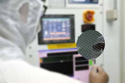 laboratory functions into a tiny integrated circuit. These chips are extremely small, typically just a few square centimeters, and are designed to perform high-throughput screening, automation, and other processes. They can also handle very small volumes of fluid, as small as a few picoliters. Learn more about the latest lab on a chip technology.
The concept of laboratory on a chip is nothing new. The concept is the integration of several high-resolution laboratory processes onto a chip. The lab on a chip allows researchers to analyze samples on location. This method is beneficial in many ways. Fluids behave differently at a small scale, enabling researchers to control the movement and interaction of samples. They are also less likely to create waste and reduce exposure to dangerous chemicals. Hence, lab on a chip is the future of analytical science.
The miniaturized lab-on-chip devices can perform multiple laboratory processes on a single chip, requiring minimal reagents. The low-cost nature of lab on a chip makes them ideal for resource-constrained environments. These devices are also highly efficient. Several microfluidic systems have been developed and reviewed in recent years. Nevertheless, fabrication techniques are expensive and complex. However, if you're looking for an efficient, low-cost device, you'll want to consider a plastic-based one.
Biophotonic Sensor Platform for Diagnostics
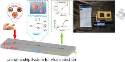
A new biophotonic sensor platform from Altug detects intact viruses. The technology 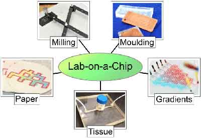 uses arrays of plasmonic nanoholes on metallic films, which transmit light at higher resonance frequencies in certain wavelengths. When a virus is present in a solution, it changes the effective refractive index of the surrounding environment, causing a detectable shift in resonance frequency. The magnitude of this shift indicates whether a virus is present in the solution.
A proof-of-concept experiment showed the viability of optical biosensors driven by co-integrated SiNOH laser. These light sources can be adapted to produce a wide range of emission wavelengths. This proof-of-concept experiment left room for improvement, as the target application for this sensor platform is point-of-care diagnostics. Hence, further improvements are required to improve its sensitivity and performance.
What is a SiNOH Laser?
What is a SiNOH laser? The SiNOH laser is a high-frequency pulsed laser that emits light at 523 nm. Its  wavelength is determined by the Nd:YLF wavelength and its repetition rate is 20 Hz. The laser's emission characteristics include a clockwise and counterclockwise-propagating mode. The GC1 and GC2 modes confirm the output power.
The SiNOH lasers are co-integrated onto a Si3N4 biosensor, which is placed in a cartridge for robust handling. The Si3N4 biosensor includes a microfluidic chamber formed by the chip surface and the cartridge lid. The laser emits light from an external source to illuminate the array of on-chip sensors. The resulting light is captured by a camera or readout window.
The Chinese name of the SiNOH laser is "Zai Ben Wen Zhong." It is based on spiral Si3N4 waveguides with dye-doped organic cladding. In addition to being based on Si3N4, it can be used as a biosensor for detecting the presence of various pathogens. This method is ideal for mass-production and can be manufactured in bulk quantities.
The researchers have developed a prototype of the biomarker sensor and are now evaluating it for clinical use. They are integrating three biomarkers into the sensor: C-reactive protein, which indicates bacterial inflammation in the body. Other biomarkers are lipocalin-2, which is a potential marker of kidney failure, and tumor necrosis factor, which is elevated in some diseases, such as arthritis or diabetes.
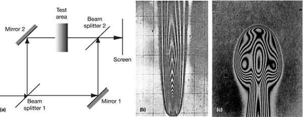
Developing a biophotonic sensor platform for diagnostics is a complex process. It involves a complex system of sensors. Each sensor section consists of three Mach-Zehnder interferometers that use light from an external source. In this way, they can detect the presence of a target molecule with greater accuracy than conventional methods. The sensor platform has the potential to revolutionize the diagnostic field and save lives.
What is Mach-Zehnder Interferometers?
If you are wondering what is Mach-Zehnder and what it does, you are not alone. Thousands of people are curious about these scientific instruments. They are used to study the relative phase shift variations of collimated beams of light, allowing researchers to study various phenomena such as particle collisions. These machines also split light from one source and analyze the differences between them. To learn more about these instruments, keep reading!

The basic principle behind the interferometer is to measure the phase shift of light from thin samples placed in an X-ray source. The samples are placed in the D and U beams, and their interaction with each other alters the phase relationship between them. This prevents destructive interference between the beams when the sample is placed in the middle. The phase shift of the sample is calculated by measuring the relative amount of light that enters each detector.
The Mach-Zehnder interferometry technique has many applications in physics, including analyzing the phase shifts of collimated beams. These interferometers can be used in a variety of applications including spectroscopy, quantum entanglement, quantum computation, neutron diffraction, optical telecommunication, and photonics. They are also useful in detecting the power of low-power lenses.
A Mach-Zehnder interferometry consists of two mirrors with an extended source and two outputs that complement each other. The two paths must be symmetrical to produce equal-length light. If they do not, constructive interference occurs in one detector, and destructive interference occurs in the other. However, equal-path conditions are difficult to obtain, so there will always be a p phase shift.
What is the Miniaturized Laboratory Procedure
A lab-on-a-chip technology is a high-tech device designed to reduce the size of traditional laboratory equipment. A miniaturized laboratory procedure on a chip uses microchannels to analyze blood samples at much lower volumes than traditional labs. This technology can also be used to integrate multiple functions into a single device, such as blood flow. Researchers from Brigham Young University and UC Santa Cruz have developed a silicon-based molecular detection platform. In an effort to develop miniaturized laboratory procedures on a chip, they have created a journal titled Lab on a Chip.
The development of lab-on-a-chip devices has been driven by advances in nanotechnology. One such advancement involves stereolithography, a manufacturing process that creates 3D objects. This method can be used to create intricate 3D architectures to manipulate the flow of liquids in LOC devices. While LOC devices are the most advanced laboratory technology available today, many more are needed to reach commercial viability.
Lab-on-a-chip technology can improve global health. It can be used to create point-of-care diagnostic devices that can reduce the burden of patients by reducing the size of sample tubes. For example, in developing countries, infectious diseases often kill people. These infections may be treated with drugs at poor health clinics, but they are often undetected, causing an even larger burden on the patient. Lab-on-a-chip technology may one day make diagnostic instruments more affordable for the general public.
The advantages of lab-on-a-chip technology are many. It offers reduced sample sizes, reduced reaction times, high throughput, and portability. It also enables targeted diagnosis of a patient while they are in the hospital. Doctors will be able to prescribe the right antibiotic or antiviral to treat their patient without the need for extensive testing. The technology has a bright future in medicine. So, what are the advantages?
How Fast Do Lab on a Chip Platforms Work?
Laboratory on a chip (LOC) is a new concept that combines multiple laboratory techniques into a microchip a few square centimetres in size. It uses techniques such as microscale manipulation to exploit the rapid mixing and heating of chemicals while minimizing waste. It also uses mathematical models to analyze the density of single E cells. It has already gained attention for research in biomedical engineering, cell interaction, and sleep disorders.
In a small package, the lab-on-a-chip device can detect sickle cell disease in newborns. It includes a miniature electrophoresis test and can be used even in remote areas. Currently, about 300,000 babies are born with sickle cell disease every year, and many go undiagnosed. Sadly, many of these children die before they reach adulthood. Lab-on-a-chip technology may be the answer to this problem.
The benefits of lab-on-a-chip technology include portability and speed of assay. It can be used for point-of-care testing, high-throughput drug screening, and bioinformatics. The smaller sample size will accelerate the adoption of LOC technology. This new technology has the potential to revolutionize the medical world. The advantages are numerous and will undoubtedly continue to grow. The key to commercial success is the ability to improve the diagnostic process in less time.
Lab-on-a-chip devices have an array of unique properties, making it possible to carry out microfluidic tests with unprecedented speed. The unique structure of microfluidic chips evokes cross-flow, making it easier to mix different colored liquids. A micropump enables fast, safe, and accurate filling of these complex structures. Moreover, lab-on-a-chip devices are designed to be portable, enabling rapid testing and diagnostic procedures right at the point of care.
What is the Market for Lab on a Chip?
The Accurate Lab on a Chip (LOC) Market research report is a comprehensive compilation of key information about the global lab on a chip market. The study includes statistics on the growth of this market and the key players operating in it. It also identifies the opportunities in the market, and provides valuable insights about the future of this technology. It is the only report available that analyses the current market in such a way.
As the technology becomes more widely adopted, doctors will be able to diagnose patients more accurately and quickly than they ever could with conventional labs. During consultations, doctors can use this technology to perform hundreds of different tests, enabling them to prescribe the right antibiotic or antiviral treatment. Unlike traditional laboratory procedures, lab on a chip does not require large amounts of blood, so less expensive medical equipment is required.
The accuracy of lab on a chip is dependent on the development of nanotechnology. The process of stereolithography allows for the fabrication of complex 3D structures, which are necessary for the manipulation of liquid flow on LOC devices. In addition, it enables researchers to perform immunoassays in just a few seconds. By enabling scientists to carry out more tests in less time, labs on a chip can significantly speed up the testing process.
In the medical sciences, early diagnosis of disease is crucial in saving lives. Early treatment of cancer and heart disease has improved survival rates. Accurate lab on a chip can help doctors identify early warning signs of these diseases. The new technology integrates several laboratory functions on a single chip. These microchannels can handle picoliters of biological fluid and separate different components. Once separated, these components can then be taken to a lab for analysis.
Are Lab on a Chip Platforms Affordable?
Lab-on-a-chip technology may improve global health by creating point-of-care testing devices. Developing countries have high rates of infectious diseases, many of which can prove fatal. While poor healthcare clinics may have drugs and diagnostic tests, they are often insufficient. Lab-on-a-chip technology could offer these nations access to affordable diagnostic instruments. But how will this technology be used? And will it benefit the global health community?
Ultimately, the cost of lab on a chip may have a profound impact on patient health. With low-cost sequencing technology, clinicians can sequence a tumor's DNA, identify mutations, and recommend individualized treatment plans for patients. As cancer treatments become more expensive, lab-on-a-chip technology could be used to diagnose it at an early stage. Because tumor cells can be detected in a patient's bloodstream, it could also aid in early diagnosis.
A miniaturized device with multiple functions, called a lab-on-a-chip, can measure various levels of lead in sediments and water. This innovative technology could help municipalities, water companies, schools, and homeowners test for lead in their water and soil. The researchers' research was published in the IEEE Sensors Journal. The device could potentially be used in a variety of applications, including environmental monitoring and drug development. The researchers hope to see the technology become a reality in the near future.
The development of lab-on-a-chip technology started about 30 years ago. The military is investing heavily in the technology because it could help detect biological threats early. This technology is so valuable that it has been dubbed "lab-on-a-chip".
Video: Lab-on-a-Chip Explained
Advantages of a Silicon Wafer for Lab on Chip
In the laboratory on chip system, a silicon wafer is patterned using dry etching and lithography. Its structure is then sealed using glass. On its back, it has fluidic connections to reagent reservoirs and outlets. The resulting system is able to work with various reagents. Here are a few advantages of silicon-based lab on chip systems.

Electrostatic Chuck Face
The Electrostatic ChuckTM is a specialized tool used for holding a silicon wafer or mask in sub-atmospheric operations. It is made up of an insulator block that has a planar surface and at least one electrode. The electrodes are connected to a source of voltage, and a support base is attached to the insulator block. An electrostatic shield ring member is positioned around the outer perimeter of the insulator block.
The chuck face is used to hold the silicon wafer during the etching and singulation portions of the dicing process. A low-pressure helium thermal-contact gas is also used during the process. This gas helps to remove heat during the plasma etching step. The chuck face is then covered with patterned mask. A bipolar electrostatic chuck supports a portion of the backside of the substrate carrier, allowing the gas flow through it.
A Sandia design uses an electrostatic chuck face to hold the silicon wafer. This surface supports the wafer, allowing it to dissipate the heat generated by the plasma. The material used in the chuck face is electrically-conductive, but it must be low enough to prevent leaks and short circuits. If the chuck face is too electrically-conducting, it could short the power supply and introduce a time delay.
The electrodes in the electrostatic chuck clamp onto the silicon wafer and control the temperature with a confined helium gas. The electrodes are made of a high-purity, highly conductive AlN and ceramic materials. They are also highly resistant to a range of oxidizing and reducing metals. With these materials, they can reduce alkali metals to a few ppm and still maintain a high degree of purity.
High AspectRatio Structures in Silicon
In the process of developing a high aspect-ratio semiconductor device, a single silicon wafer was etched through three semicircular gaps at a uniform rate. The etch rate was reduced as the depth of the high-aspect-ratio structure increased, indicating that the etched layer is not completely flat. A subsequent step involved retracing the etched layer with a one-wt% HF solution at room temperature for 22 min. The etched layer served as a protective layer for the bulk silicon substrate.
To achieve high aspect ratio structures in silicon, an improved Bosch etching process was used. This process, which is widely used to fabricate high-aspect-ratio Si structures, relies on a switch between passivation and isotropic etching. A cavity with straight sidewalls is obtained through this technique. This process has been adapted and refined by Hirose et al.
This technique produces high aspect-ratio structures by introducing corners with appropriate geometry. The process can be repeated over, enabling miniaturization. Moreover, the multistep plasma etching process results in a high aspect-ratio silicon wafer. Furthermore, the residual polysilicon layer remains in the etched silicon after the final etching step, which enables it to achieve a high-aspect-ratio structure.
The high aspect-ratio structure is fabricated by coating the silicon nanostructures with 250 nm a-C-N-H and two mm of SiO2. The resulting structure is not completely conformal and there are voids between the silicon nanostructures. This process has been used for fabricating nanochannels. Because of its high aspect-ratio structure, this process requires careful consideration of membrane thickness. The relationship between thickness and pitch must be carefully studied when designing the membrane for high-aspect-ratio structure.
Uniformity
Optimal wafer thinning can make the overall yield of your device higher. High open area wafers are notoriously difficult to process due to loading effects and uneven etch depths. Large differences in etch depths can render certain dies unusable and reduce your overall yield. For this reason, the best way to make the thinning process as uniform as possible is to use a template that specifies the exact edge profile of the wafer.
A common commercial wafer is 375 um thick. Thermal oxide is grown on the top of the wafer to define the confinement dimension. A pattern is etched in the oxide by lithographic processes. Next, the wafers are cleaned in RCA solutions and rinsed with deionized water. After the cleaning process, the wafers are bonded and annealed at about 1,100 degC.
The Nanyang Technological University researchers developed a technique to create uniform semiconductor wafers. This new process could help manufacturers combat the chip shortage currently affecting the industry. The Covid-19 pandemic has resulted in an acute shortage of silicon chips. Typically, semiconductor chips are fabricated on silicon wafers and then diced up into tiny chips. While the process is generally reliable, it can also produce defective chips, which increases the cost of manufacturing.
Another process that has become increasingly important is thin film deposition of different materials on the surface of the silicon wafer. The integration of the three-dimensional structures is creating new challenges for deposition processes. One key challenge is uniformity of the layers. Optimal uniformity requires control over temperature, gas flow, and layers. It is imperative to use a process that produces uniform layers over the entire wafer.
Scalability
A recent study showed that nanotransfer printing on silicon can achieve 99.98% yield transfer of a 20-nanometer thick Au film onto a six-inch silicon wafer. While the study was limited to a laboratory setup, the researchers believe that this technique can scale to a twelve-inch silicon wafer, which is the mainstream size of silicon wafers used by semiconductor chipmakers. The key to success of this technique is the uniformity of the printed metal layers and their scalability.
To develop a scalable semiconductor wafer, researchers from the Nanyang Technological University and the Korea Institute of Machinery & Materials developed a technique that would make a uniform silicon surface. The new technique could lead to higher chip yields and more cost-efficient semiconductors. The fabrication process of semiconductor chips is time-consuming and requires special environments. A single silicon wafer can contain thousands of chips, or only a few dozen.
Traditional chip scaling is not as easy as it used to be, and the semiconductor industry is laying plans for 5nm and beyond. The problem is that the benefits of scaling diminish with each successive node. This is a problem that chipmakers are trying to solve by exploring less conventional approaches such as advanced packaging and in-memory computing. Some of these methods are already available, while others are still in R&D.
Etching
Several different approaches are available to etch silicon wafers for lab on chip applications. The most commonly used method involves anisotropic wet etching. This method produces rounded depressions on the wafer's surface that undercut the masking layer. The rate at which materials are etched varies depending on the crystal planes and acid concentration. This method is 100 times faster than anisotropic etching.
Wet etching is an alternative method of etching silicon. In this method, the substrate is partially covered with a protective coating and immersed in an etchant bath. There are many different etchants available, and each one requires a masking material. Etching rates depend on the concentration of etchant, and a higher concentration causes the silicon to etch more slowly than a lower concentration. In addition to etchant concentration, water acts as an oxidizing agent for silicon.
Anisotropic wet etching involves selectively etching silicon at different crystallographic planes. This method requires the use of an aqueous potassium hydroxide solution with a concentration of 20% or higher. The concentration of KOH must be high enough to ensure good etching. Low concentrations can produce rough surfaces and insoluble residues. An additional consideration is the possibility of introducing boron-doped silicon in the etching process.
Microfluidic fabrication techniques such as soft lithography and thermoforming are also possible. The method of choice will depend on the substrate, available equipment, and desired functions. The first step is to clean the silicon wafer. Then, a barrier layer is applied. Next, a photoresist coating is applied to the surface. The photoresist is spun at a high speed to enable a clear definition of the thickness. Finally, the solvents must be removed from the exposed surface.
What Substrates are Commonly Used to Fabricate a Lab on a Chip
In lab-on-a-chip (LOC) technology, various substrates are used depending on the desired properties, fabrication techniques, and application requirements. Some of the most commonly used substrates in LOC devices include:
-
Glass: Glass is a popular substrate due to its excellent optical properties, chemical resistance, and biocompatibility. Glass substrates are often used in applications that require high-quality optical imaging or precise surface patterning. However, glass can be more difficult and expensive to process compared to other substrates.
-
Silicon: Silicon is a widely used material in the microelectronics industry and has been adapted for use in microfluidic devices. Silicon offers good mechanical strength, thermal stability, and chemical resistance. However, it is relatively expensive and can be challenging to process for some applications.
-
Polymers: Polymers are widely used in LOC devices due to their low cost, ease of fabrication, and broad range of material properties. Commonly used polymers include polydimethylsiloxane (PDMS), polymethyl methacrylate (PMMA), polycarbonate (PC), and cyclic olefin copolymer (COC). Each polymer has its advantages and limitations, such as biocompatibility, optical transparency, and chemical resistance.
-
Paper: Paper-based microfluidic devices are gaining popularity due to their low cost, ease of fabrication, and disposability. Paper substrates can be functionalized with hydrophilic and hydrophobic regions to create channels and reservoirs for fluid transport. These devices are particularly suited for point-of-care diagnostics and resource-limited settings.
-
Hydrogels: Hydrogels are a class of materials that can absorb and retain large amounts of water. They can be used as substrates in LOC devices, particularly in applications that involve cell culture and drug delivery. Hydrogels offer advantages such as biocompatibility, tunable mechanical properties, and the ability to mimic the natural cellular environment.
Each substrate has its unique advantages and challenges, and the choice of material depends on the specific requirements of the LOC device and its intended application.
Can Germanium on Insulator (GOI) Substrates be Used to Fabricate Lab-on-Chip Devices?
Germanium-on-insulator (GeOI) substrates can be used in lab-on-a-chip (LOC) devices, although they are less common than other substrates like glass, silicon, or polymers. GeOI substrates are mainly used in microelectronics and optoelectronics due to their unique properties, which include high carrier mobility, strong light absorption, and compatibility with silicon-based processes.
GeOI substrates could be employed in LOC devices requiring integrated electronics or optoelectronics, such as sensors, actuators, or optical components. The main advantage of using GeOI in these applications is the possibility of achieving high-performance devices with increased speed and sensitivity.
However, some challenges are associated with using GeOI substrates in LOC devices. Germanium is more expensive than silicon, and its fabrication processes are generally more complex. Additionally, the biocompatibility and chemical resistance of GeOI substrates has yet to be extensively studied compared to more common LOC substrates.
In summary, while GeOI substrates can be used in lab-on-a-chip devices, their adoption needs to be improved due to the higher costs and complexity of fabrication and the lack of extensive research on their suitability for various applications. They might be more suitable for specific use cases that require the unique properties of germanium, such as integrated optoelectronics or high-speed electronics.
Germanium on Silicon (GeOSi) Substrates for Lab-on-a-Chip Device Fabrication
Germanium-on-silicon (Ge-on-Si) is a semiconductor material system in which a thin layer of germanium (Ge) is epitaxially grown on a silicon (Si) substrate. This combination is primarily used in microelectronics and optoelectronics due to its desirable properties, such as high carrier mobility, strong light absorption, and compatibility with conventional silicon-based fabrication processes.
In the context of lab-on-a-chip (LOC) devices, Ge-on-Si could be used for applications that require integrated electronics or optoelectronics, such as sensors, actuators, or optical components. The main advantage of using Ge-on-Si in these applications is the possibility of leveraging the unique properties of germanium while still benefiting from the well-established silicon-based fabrication techniques.
However, some challenges are associated with using Ge-on-Si substrates in LOC devices. The fabrication process for Ge-on-Si can be more complex and expensive compared to pure silicon substrates. Additionally, the biocompatibility and chemical resistance of Ge-on-Si substrates has not been as extensively studied as other more common LOC substrates like glass or polymers.
In summary, while Ge-on-Si substrates can be used in lab-on-a-chip devices, their adoption may be limited due to the higher costs and complexity of fabrication and the lack of extensive research on their suitability for various applications. Ge-on-Si might be more suitable for specific use cases that require the unique properties of germanium, such as integrated optoelectronics or high-speed electronics.
A researcher asked the following questions:
Questions:
I would like to get a quote for 10 Ge-on-Si (GeoSi) wafers. I would like 4 inch wafers with the following Ge thicknesses:
- 4x 2um thick layer of Ge
- 4x 3um thick layer of Ge
- 2 x 5um thick layer of Ge
If possible, I would prefer no doping in the Ge. Otherwise, I would prefer a minimum amount of n-type doping.
Can you give me the following information:
- Thickness of the Si (525um would be perfect, but other thicknesses would be fine).
- Variation in the uniformity of the thickness of the Ge layer.
Answers:
- As per the Ge layer was thick,can you accept qty. more a little each item 5pcs? thick epi layer with too small qty. is not feasible.
- We can do and do well on no doping in the Ge layer
- We can using Silicon substrate thickness at 525um
- Variation in the uniformity of the thickness of the Ge layer --> the thicker the larger variation,like as while the Ge layer thickness at 1um,the Unif=1.469%,while the Ge layer thickness 2um,the Unif =2.43%,this was the measurements we had ever measured before,fyi.
Pls see below for our offer on 100mm dia. 2um and 3um GeOSi wafer
- 2um Germanium on Silicon wafers,crystalline germanium on silicon
Si wafer: 100mm, P-type, <100>, thickness 525+/-25um,Resis. 1~20 Ohm.cm
Ge layer: Un-doped 2 um thick, good crystalline and uniform,un-polished
Qty. 5 wafers.
- 3um Germanium on Silicon wafers,crystalline germanium on silicon
Si wafer: 100mm, P-type, <100>, thickness 525+/-25um,Resis. 1~20 Ohm.cm
Ge layer: Un-doped 3 um thick, good crystalline and uniform,un-polished
Qty. 5 wafers.
Reference #245401 for specs and pricing.

 laboratory functions into a tiny integrated circuit. These chips are extremely small, typically just a few square centimeters, and are designed to perform high-throughput screening, automation, and other processes. They can also handle very small volumes of fluid, as small as a few picoliters. Learn more about the latest lab on a chip technology.
 uses arrays of plasmonic nanoholes on metallic films, which transmit light at higher resonance frequencies in certain wavelengths. When a virus is present in a solution, it changes the effective refractive index of the surrounding environment, causing a detectable shift in resonance frequency. The magnitude of this shift indicates whether a virus is present in the solution.
 wavelength is determined by the Nd:YLF wavelength and its repetition rate is 20 Hz. The laser's emission characteristics include a clockwise and counterclockwise-propagating mode. The GC1 and GC2 modes confirm the output power.