What is a Silicon Boule?
A Silicon boule is a cylindrical rod made by melting a mixture of 8 sands and 8 charcoals in a blulectric alloy furnace. Several methods have been used to produce Silicon boules, but two of the most common are the Czochralski Process and Bridgeman Technique. Most of the Silicon crystals grown for use in producing electronic circuits are produced using the Czochralski process (CZ-Si), as the Czochralski process is the least costly available method and is able to produce crystals with larger sizes.
When it comes to manufacturing electronics, Silicon Boules are an excellent material to work with. They are not to be confused with the GregTech Silicon Cell, which is used in the making of Solar Panels. They can also be created by using a Blulectric Alloy Furnace and 8 Coal. A Diamond Handsaw is used to cut the Boule into wafers. If you want to produce your own solar panels, the process is very simple.
What is the Bridgeman Technique and the Stockbarger Method
The Bridgeman technique solidifies melts from a hot zone to a cold zone. The polycrystalline material in  the crucible must be melted and brought into contact with a seed at the bottom of the crucible. The process involves the addition of new atoms, ions, and polymer strings to the melt, which results in the formation of a single crystal. Typically, crystalline solids have high Young's modulus and high shear modulus.
This process produces large single crystals, called boules. The most perfect of these crystals is silicon, which is found in nature. The Stockbarger method produces monocrystalline ingots, which can weigh more than two hundred kilograms. It is similar to the Bridgman technique, but uses slightly different cooling systems. The Bridgeman method solidifies a solid ingot by heating a mixture of silicon, carbon, and alumina.
The Bridgman technique uses a two-zone furnace to grow synthetic boules. The materials must be stable during the process and must not undergo phase transformations or decomposition before melting. It is important to have a conical-shaped ampoule and a suitable gradient to promote growth. Using the Bridgeman technique requires a crucible that is translated along an axis that corresponds to the furnace's temperature gradient.
The Bridgman technique is a technique used to grow single crystals in a controlled environment. The temperatures in the system can be varied by varying a specific temperature. The resultant single crystals are often used in electronic devices. In some cases, the crystals may be useful in a semiconductor. However, some scientists are skeptical that the Bridgman technique will lead to more reliable results. The process is not yet widely available and more research needs to be conducted before it can be considered a viable alternative to the other methods.
Video Bridgeman Technique
A silicon boule is a cylindrical rod that is made by melting a mixture of 8 Sand and 8 Coal in a Blulectric Alloy Furnace. The resulting boule can be cut into 16 smaller ones. They are a valuable and versatile material that is used in many applications, such as solar panels. So, if you're looking for a durable, inexpensive way to make a solar panel, silicon is a great choice.
A silicon boule is the starting material for most integrated circuits. A silicon boule is formed by using synthetic methods. The Czochralski process requires a seed crystal, which is melted into pure molten silica. The molten silicon grows on the seed crystal in a crystalline pattern. Once solidified, the resulting silicone is a semiconductor. In a computer, a Silicon Boule can be used as a capacitor, transistor, or in a memory chip.
These crystals are the basic starting material for most integrated circuits. These crystals are created in several ways, and the Czochralski process is the most common. It involves pulling a seed crystal from molten silicon and forming it into a cylindrical ingot, called a boule. The resulting silicon is then used in electronic circuits. The shaper is responsible for the shape of the boule. The Czochralski process also uses a silicon seed crystal.
Silicon boules are the starting material for most integrated circuits used today. These crystals are the best option when it comes to a silicon implant. These are used to form the chips used in smartphones and other electronic gadgets. They can also be used in semiconductor manufacturing. They are made in high-tech factories. In the past, they were only used for making lasers, but today, they are essential for semiconductor production. A single silicon boule has a diameter of about 6 inches.
Silicon boules are single-crystal ingots. The largest ones are 6 inches in diameter and contain nine creases. They were discovered in the back room of a mineral dealer's shop in California. Sadly, the owner of the shop died before they were discovered. They are very rare and extremely valuable, so it is important to understand what they are and why they are used in technology. When you're making an electronic device, you need a silicon boule.
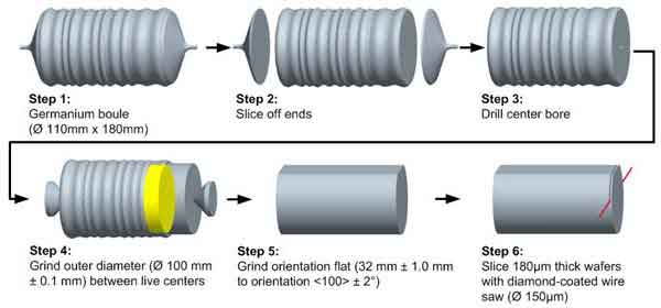
How Are Boules Sliced Into Semiconductor Wafers?
There are several ways to create boules: annealing, laser cutting, and wire-sawing. In some factories, up to  100 blades are used. Laser cutting allows the process to be faster and more precise. Sawing is also a common method for cutting wafers.
Processes for creating boules
One way to make a boule is to use flame fusion. Flame fusion involves providing a continuous flow of solid raw material, usually in powder form, to a hot flame. The solid material is then projected against a receiving surface and solidifies. This process can be done at a high or low aspect ratio, depending on the desired outcome.
The boules that are created with this method have flats and minor flats on their surfaces. The flats are usually located in the cleavage plane. The process begins by turning a boule of silicon to a diameter of about two inches. This process creates a cylinder that has a front and back face, and an outer peripheral edge 230. A major flat 240 is ground into the edge of the boule along the 22-4 plane family. The flats are then sliced into individual wafer blanks.
The next step is to find a suitable substrate. A suitable substrate is important in creating high-quality boules. If you want to make monocrystalline boules, you need a substrate that is compatible with nitrides. For this process, a silicon wafer has to be coated with a photosensitive material, called a photoresist. A bright light is then shone through the photomask, causing the photoresist to soften.
The yield rate of semiconductor devices produced using this process is typically on the order of 25% to 30%. However, some embodiments have demonstrated yields of up to 100%. Another advantage of this method is that it allows for flexible processing of the boules without annealing. Furthermore, the boules are processed with increased cooling rates.
In addition to improving yield, embodiments of the present invention provide a high-quality single-crystal spinet boule. This method has the advantage of being cost-effective, and can significantly reduce the thermal budget of the entire fabrication. It also allows for increased throughput and lower manufacturing costs.
Silicon boules are a common starting material in most integrated circuits. They are used in semiconductor manufacturing, as well as in the manufacturing of other electronic gadgets. For instance, they are an excellent material for solar panels.
Single crystal spinel boules
Single crystal spinel boules are generally triangular in shape with twelve facets. The facets are oriented along two planes, the 22-4 and 02-2 planes. These facets are characterized by their different sizes and orientations.
A single crystal spinel wafer has a crystallographic orientation represented by a general formula aAD*bE2D3, where A and E are chosen from a group of metals. When the ratio b:a is greater than 1:1, the spinel is rich in E2D3.
The process involves a cutting tool that can slice through a boule into a wafer. One option is to use wire saws to cut the boule. This method has some advantages over photonic equipment, including a low yield rate.
Single crystal spinel boules are typically grown by the Czochralski technique. The top and tail are then removed from the boules. These boules are then x-rayed with the Laue backscattered technique in order to confirm their orientation and identify the front-side of the wafer. This method also helps determine the approximate position of the major flats.
EFG crucibles are generally hollow and less susceptible to wear and melt volatilization. In addition, they are typically cut to their final diameters, which reduces the amount of material that must be removed during grinding and polishing. This is because the EFG crucible is molten for a much shorter period of time.
The total cost of this crystal growth process is $159/wafer. This cost includes the cost of energy and labor, the use of the photonic equipment, and the cost of the materials consumed during the process. The material cost of the process is the seed crystal and the Ga2O3 powder.
The cleavage plane is parallel to the major flat and intersects the front face of the boule at a point. The cleavage plane also intersects the back face with a line. The back face has a more negative slope than the front face. The angle between the front and back faces is generally around forty to sixty degrees.
During the manufacturing process, single crystal spinel boules are exposed to a batch of melt. The seed crystal is typically made of stoichiometric spinel that has sufficient parity and crystallographic homogeneity to grow into a boule. During the process of boule growth, the seed crystal may be rotated relative to a fixed crucible. This rotation draws out the seed crystal.
Single crystal spinel wafers
The first step in growing boules is to slice the single crystal spinel wafer using the Czochralski technique. The boules are then x-rayed using the Laue backscattered technique, ensuring that they are oriented in the correct direction. The next step is to grind the major flat 240 into the edge 230 along the 22-4 plane family. This step may be performed before or after slicing, depending on the needs of the process.
The process can also be used to identify the orientation of a boule. The backscattered electrons of a Laue camera are used for this purpose. The images show various orientations of the spinel, which can be used for further analysis.
The first step of the process is to slice the single crystal spinel wafer into pieces that are approximately the same size. This is an important step in the production of spinel, as it makes it easier to cut. However, this process is not always easy. It requires complex equipment and requires expertise in the use of photonic equipment.
After this step, the boule is sliced into boules using photonic equipment. In addition to this step, a single crystal boule can be processed by using the Czochralski pulling technique. This technique can be used for the formation of boules of stoichiometric spinel. A single crystal boule typically has a process aspect ratio of 0.39.
During the process of cutting single crystal spinel wafers, the outer periphery has a flat that indicates the orientation of the cleavage plane. This plane is usually oriented along the plane family 11-2, and extends outward from the front face. A second flat on the outer edge indicates the direction of cleavage propagation.
Single crystal spinel wafers are fabricated using a process that promotes single crystal growth during the fabrication of melt growth semiconductors. During the process, the semiconductor source material in the growth ampoule is placed in a first thermal environment. Then, the material is transitioned to a second thermal environment. This transition causes the semiconductor source material to attain a temperature below its solidus temperature. Single crystals are then mechanically perturbed, which promotes growth.
This process yields large sapphire boules with low bulk absorption at 1064 nm. The wavelengths of the crystals can be adjusted to ensure that they have very small absorption values and low levels of birefringence. In addition, LAOS crystals are an excellent material for HEL applications due to their low temperature coefficient of refractive index.
Photonic equipment
The manufacturing process for semiconductor devices is a complex sequence of steps requiring near perfection and high precision. If one of these steps is missed, it can result in device-killing defects. The MKS Handbook of Semiconductor Devices and Process Technology describes these steps in detail. Precision photonic equipment helps in inspection and metrology, two critical areas of semiconductor manufacturing. The process steps are illustrated in Figure 5 and summarized in Table 1.
First, boules are annealed and sliced to create wafers. The thickness of the wafer depends on the material used. In general, GaAs wafers are 25 mils thick, while InP, SiC, and sapphire wafers are a bit thinner. Wafers can be sliced using laser, wire-sawing, or sawing equipment. Some factories employ 100 blades or more to achieve the precision required for these operations.

 the crucible must be melted and brought into contact with a seed at the bottom of the crucible. The process involves the addition of new atoms, ions, and polymer strings to the melt, which results in the formation of a single crystal. Typically, crystalline solids have high Young's modulus and high shear modulus.
 100 blades are used. Laser cutting allows the process to be faster and more precise. Sawing is also a common method for cutting wafers.