Silicon Fabrication Methods | UniversityWafer, Inc.
Silicon Material Breakdown
Silicon material ranks as the world’s second most common element. In the entire universe, it stands as the seventh most abundant element. In the semiconductor world, this material has been embraced to be used in the technology and electronic sector. Five main silicon fabrication methods do exist and have been illustrated below. Silicon is important as it acts as a substrate in micro electric devices. The most common use of silicon wafers is in making integrated circuits that power our devices.
Buy Your Wafers Online and Save!
Get Your Question Answered FAST!
Silicon Fabrication Methods
Silicon fabrication methods include Photolithography, Thermal oxidation, and Layer transfer techniques. All of these methods require a mask, and require repeated steps to create a transistor pattern and openings. After these steps are completed, the transistor regions are metallized. The subsequent steps define the pattern of contacts on top of the oxide.
- Photolithography
- Silicon Carbide Grinding Agent
- Thermal Oxidation
- Layer Transfer Technique
Photolithography
Photolithography is one of the most complex fabrication processes used for semiconductor devices. It uses light as an etching medium to transfer a design onto a silicon wafer. As transistors continue to shrink, this method is especially useful for building ultra-small transistors. It also limits the amount of high-resolution areas and geometries that can be built. This process requires a clean room environment.
This process is often used for computer chips. The process can produce hundreds of microchips on a single silicon wafer. The technique requires a very clean environment, and it is extremely difficult to damage the wafer. However, it is an indispensable step in the fabrication of computer chips.
Despite the many advantages of photolithography, it is not without its disadvantages. The process can cause silicon atoms to form silicon dioxide. Silicon dioxide is the result of a chemical reaction between oxygen and silicon. The reaction starts at room temperature and stops when a thin oxide film has formed on the surface. The resulting silicon dioxide layer is a good insulator, and also a mask for ion implantation. This property of silicon is the primary reason why it is still the dominant material in IC fabrication.
Soft lithography is another fabrication method that is extremely versatile. This method is particularly useful for fabricating microfluidic devices. It is also cheaper than photolithography and can produce high-resolution micropatterns in less than 24 hours. This method of semiconductor fabrication is particularly popular with semiconductor manufacturers, who need to produce high-quality chips quickly and at low costs.
Soft lithography is another technique that is rapidly catching on. While soft lithography is low-cost, it is not easy to produce complex designs. SU-8 is often used as a mold material, and it comes in many different thicknesses. The resulting molds can be highly accurate.
A second method of fabricating silicon wafers is called reflow. In this process, a silicon wafer is anodically bonded to a silicon oxide layer. This layer is formed through a wet thermal oxidation process. The resulting silicon-glass wafers are then mechanically lapped and polished.
SiC grinding agents
Polycrystalline silicon carbide is a widely used material in the ceramics industry for a variety of applications. Its refractory and mechanical properties make it a good choice for grinding agents and high-strength machine tool coating. It is also biocompatible, exhibiting minimal tissue response. Furthermore, it can be mineralized with hydroxyapatite sol-gel coatings.
SiC grinding agents are primarily used to grind non-ferrous materials such as ceramics and carbides. These materials generally have lower tensile strength and ductility than silicon. However, the benefits of SiC-based grinding agents far outweigh the drawbacks. For these reasons, it is a popular choice for semiconductor fabrication.
SiC is also used in bone and is a useful material for biomedical applications. Beke et al. have found that SiC nanostructures can be used to treat cancer. These are just a few of the applications of silicon nanotechnology. And there are countless other applications that make it one of the most widely used materials in semiconductors.
The properties of SiC can be modified through chemical processing and by adding impurities. In the case of silicon, phosphorus and nitrogen impurities produce an N-type semiconductor. Controlled doping can also make SiC more conductive. SiC can also undergo electrical ageing, which is a gradual increase in electrical resistivity due to oxidation. If the temperature and frequency are suitable, SiC can conduct electricity under certain conditions. In addition, the conductivity of silicon depends on the voltage, intensity of ultraviolet rays, and infrared radiation.
The process of silicon fabrication requires optimum grinding parameters. The temperature of the grinding zone is highly elevated as the grinding depth increases. The resulting temperature decreases the surface roughness and improves the fracture toughness of the silicon carbide. If the grinding depth exceeds fifteen millimeters, the surface quality will gradually improve.
SiC is a synthetic compound of silicon and carbon. It has a hardness rating of nine on the Mohs scale. Its high hardness makes it useful for cutting and grinding products. Its low thermal expansion and refractory properties make it an excellent choice for high-temperature bricks. It is also classified as a semiconductor, which is why it is used in many high-tech products.
Thermal oxidation
Thermal oxidation as a silicon fabrication process involves the oxidation of silicon, oxygen, and heavy metal ions. In this process, the native silicon layer is removed and replaced with a desired oxide. The oxide layer is necessary for the lithography process and provides passivation. Besides providing a protective layer against oxidation, it also fills vacancies in the silicon crystal that are not present in the interior.
Thermal oxidation is one of the major steps in the fabrication of semiconductor chips, and the success of an IC manufacturer depends on the ability to grow an oxide film with a uniform thickness. Water vapor is commonly used for the oxidation process, and new steamer designs replaced water bubblers, direct water injection, and pyrolytic torches. This new steamer method offers several advantages over traditional water-vapor delivery methods, including cost reduction, safety, and improved film uniformity and growth rate.
The chemical reaction that occurs on a silicon wafer is limited by the number of silicon atoms available. As the oxidation temperature increases, oxygen atoms must diffuse longer distances in order to react with the silicon. This causes the thickness of the oxidized layer to increase, but the rate of growth is self-limiting at a particular oxidizing temperature.
Thermal oxidation can also be applied to different materials. However, most commonly, it is used for oxidizing silicon substrates. The process uses a quartz glass carrier and multiple chemical supply pipes. During the oxidation process, the wafer is heated to 1000 degrees Celsius.
The process involves heating a silicon wafer to a high temperature. The oxygen in the oxidation process reacts with the silicon, forming a layer of silicon dioxide. This process produces thin layers of oxide and is the preferred method for thick oxides. The silicon in this process is consumed in the oxidation process, about 45 percent of the silicon that ultimately makes up the final layer.
A two-step thermal oxidation process improves the uniformity of the thin oxide layer in semiconductor wafer fabrication. This improvement is reproducible from run to run. Compared to one-step thermal oxidation, the two-step process also minimizes the uncontrolled formation of the oxide layer and results in a substantially uniform final layer thickness.
Layer transfer technique
A layer transfer technique is a fabrication process that introduces controlled amounts of impurities into a silicon crystal. Often, this is done through predeposition, where a semiconductor substrate is heated to a controlled temperature and excess dopant is provided. The dopants then diffuse into the crystal until they reach a maximum concentration. This concentration depends on the temperature of the wafer, which is high enough to allow a larger amount of dopants to diffuse into the crystal. The amount of time it takes for the impurities to reach solid solubility also determines the amount of dopants that are introduced into the crystal.
The process is often followed by performing nanoimprint lithography on a silicon wafer. This involves a silicon imprint mold, which has pillars with a 300-nm pitch. The mold then etches the silicon layer under 40 bar for about five minutes at a time. The silicon layer is then transferred to a flexible PDMS substrate.
Another type of layer transfer technique is CVD. This technique is an indirect method for patterning a silicon wafer. It involves depositing a substance onto a silicon wafer using a chemical slurry. This creates a flat, plane surface that is necessary for lithography and pattern transfer. The process starts at the higher regions of the wafer, and leaves defined lower lying regions untouched.
The HIT cell is a simplified example of this technique. A similar cell design is shown in Figs. 21-23. This shows the design and processing details. This fabrication technique involves depositing a thin film of silicon onto a hot substrate. During the process, an additional backing handle wafer is used to protect the front surface of the silicon wafer.
After silicon oxidation, a silicon dioxide layer is deposited on the wafer. This layer controls the amount of dopants that can enter the silicon. It is essential to ensure that the layer is thick enough to prevent impurities from entering the silicon. Once deposited, the silicon dioxide layer can be used as an insulator and as a mask for ion implantation. This property of silicon is a key reason why silicon has a dominant role in IC fabrication.
Soi wafers are similar to SDB-SOI wafers, but they are not the same. The process is called "smart cut" and involves an oxidized silicon wafer with a silicon film on top. The resulting wafer is bonded to a substrate and annealed at 400-600 degrees C. The thickness of the resulting wafer is limited to a few microns, due to ion penetration depth.
Silicon Wafer Fabrication Techniques
a. Bridgman Method
This method is based on directional solidification as a result of moving molten silicon from a hot area to a cold section slowly in a furnace. This method is achieved either in horizontal system setup or a vertical system arrangement. The idea behind the two techniques is fairly similar. It should be noted that crystals obtained from the horizontal approach will have better crystalline qualities as they have low dislocation densities as a result of reduced stresses. This is because the free surface of the melted top can expand freely in the course of the growth process (Avadhanulu M.N. & Murthy).
(I). Vertical Bridgman Method
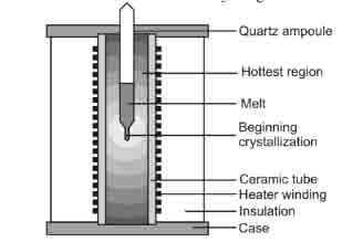
The powder material is introduced into a sealed quartz-based crucible. The sealed crucible has a vacuum inside and is placed inside the Bridgman furnace. The crucible is heated such that the powder inside completely melts and the hot zone is in contact with the seed at the bottom. The seed is a single crystal item that grows following a specified crystallographic orientation. A section of the seed remelts thus aiding crystal growth on the newly formed interface. At this point, the crucible has to be slowly shifted to a cooler section of the furnace. Since the temperatures present at the bottom end of the crucible are way below the solidification temperatures, crystal growth has to be initiated by the seed. This takes place at the interface of the melt and the seed. The entire melt will solidify to a single crystalline ingot given that the crucible has been moved through the cold zone. This whole process will take an average of about ten to fourteen days. Crystals grown from this method do exist in a circular shape (Avadhanulu M.N. & Murthy).
Figure 1: An illustration of the Bridgman furnace. (Avadhanulu M.N. & Murthy)
(ii). Horizontal Bridgman Method
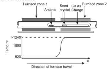
This method utilizes a two-zone furnace to obtain crystal growth. The left side zone of the furnace temperature is kept at temperatures of six hundred and ten degrees Celsius. The right end on the other hand is heated to a temperature slightly higher than the raw materials melting point. Given that movement occurs in the right to left direction, the molten raw material has to cool and solidify as a result of the movement. If a seed crystal is positioned on the left side of the melt such that only the end of the seed will melt as a result of the temperature gradient, the specific arrangement of the single crystal changes to form a purely single crystal. D shaped crystals are obtained when this method is applied (Avadhanulu M.N. & Murthy).
Figure 2: An illustration of a two-zone furnace. (Avadhanulu M.N. & Murthy)
Silicon cannot be grown by this method if silica boats are used as the solid Si sticks firmly to the boat while differential contraction breaks the crystal on cooling. However, when a water-cooled metal boat with high conductivity is used, the above limitation is overridden making it possible to grow silicon using this method.
b. The Gradient freeze method
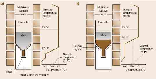
This method is almost similar to the Bridgman technique only that the temperature gradient has to be translated along with the melt to implement directional solidification. This method can be attained following a vertical gradient freezing approach or a horizontal arrangement. The crucible, melt, seed, and the furnace have to be maintained in a stationary position when this method is employed. The temperature gradient moves from the interface between the seed and the melt to the crystal end following the crystal growth direction. To achieve this, a multi-zone furnace system has to be used such that the power in each zone can be varied and controlled using individual the proportional-integral Derivative (PID) controllers. It is of the essence to use the multiple heater zones in maintaining a similar temperature gradient in the interface between the melt and the solid in the course of the crystal growth process (Govindhan Dhanaraj, 2010).

Figure 3: An illustration of the gradient freeze method. (Govindhan Dhanaraj, 2010)
The vertical gradient freeze technique is advantageous as one can achieve reduced radial and axial temperature gradients. This in turn gives room for low dislocation densities.
(I). Horizontal gradient freeze method
In this technique, the melt is solidified gradually as a result of the movement of the temperature gradient along with the melt. The staring raw materials (pure Ga and As) are held in a sealed tube where Ga is in a quartz crucible in one end of the furnace while As is positioned in the opposite further end. A porous barrier separates the two elements allowing As vapor to react with Ga. The quartz tube has to be in a two-zone furnace such that As is maintained at six hundred and twenty degrees Celsius temperature while Ga is at the range of one thousand two hundred and thirty-eight degrees Celsius and one thousand two hundred and seventy degrees Celsius temperature condition.
c. Czochralski Technique
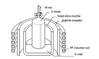
The silicon-based raw material is feed into a crucible and then it is heated to temperatures that are higher than the raw material temperature. A pull rod that has a chuck holding a seed rod at the lower endpoint is stationed right above a crucible. Then the seed crystal is sunk into the molten material and at the same time, an adjustment is made to the melting temperatures till a point is attained where the meniscus is supported by the seed crystal. Slow rotation motion of the pull rod is initiated and maintained while at the same time lifting of the rod is done slowly. The power that is supplied to melt the crystal to the desired diameter is varied such that an output desired diameter ingot is grown.
This setup is carried out in conditions that it is possible to regulate the ambient gas plus also the observation of the crystal visually. With this method, crystals with a length to diameter ratio higher than unity can be obtained. The diameter of the crystal hardly does exceed half the crucible diameter. It is however impossible to grow crystals with larger diameters as it becomes difficult to maintain a uniform crystal diameter.

Figure 4: Crystal growth using Czochralski method. (Kuphaldt, 2009)
Crystal growth References
Avadhanulu M.N. & Murthy, A. T. (n.d.). A Textbook of Engineering Physics, . S. Chand Publishing.
Govindhan Dhanaraj, K. B. (2010). Springer Handbook of Crystal Growth . Springer Science & Business Media.
Kuphaldt, T. R. (2009). Lessons In Electric Circuits, Volume III – Semiconductors.


