Silicon-on-Insulator Silicon Photonics Applications
A company founder requested the folllowing quote:
Do you ever stock high-resistivity SOI for silicon photonics? We're looking for a supplier for one or two wafers.
We need two products. The first would be 220 nm-thick silicon (100) on 2 micron oxide. The resistivity should be high (>1000 Ohm-cm). This is a standard silicon photonics stack. One caveat, we'd like the backside to be polished.
I'll get back to you on the specs of the second wafer. We're not sure yet about the thickness of the device layer, but if it came 220 nm, we could thin it. It will also be (100) high-resistivity Si but on a thin buried-oxide. 300 nm for the buried oxide would be great. This thin box is more common in electronics. We don't need a polished backside for this wafer.
Reference #273106 for specs and pricing.
SOI Devices Based on Silicon Photonics
A semiconductor engineer of a company dedicated to the development and technological products requested the following:
My team and I are developing a device based on silicon photonics, so we would like to use your SOI wafers with the following specifications: Handle wafer: 400 um (or thinner if possible) Box layer: 2um (SiO2) Device layer: 80 um (ideally 65 um) We are in the early stage of development and initially we'll be needing low volumes for running tests. We would like to know the cost of this type of product, the delivery time, and the MOQ.
Reference # 271631 for specs and pricing.
Thin Device Layer SOI to Fabricate Silicon Photonics Devices
A silicon photonics engineer requested the following quote:
We are looking to do silicon photonics, and wondering if you have the 220 nm SI SOI wafer, Stochimetric SiN 150 nm thick and LPCVD SiN 450 nm thick. All of them 100 mm in diameter with 2 or 3 um of oxide underneath. Please see below for the specs. Please let me know the cost of each. We are looking to get 2 wafers of each type to start.
Looking to purchase 220 nm thick silicon SOI wafers with the spec below: 200mm SOI WAFERS DEVICE TOP LAYER: Diameter: 200±0.2mm Type/Dopant: P/B Orientation: (1-0-0)±0.5° Thickness: 220±10nm Resistivity: 8.5-11.5 ohm-cm Flats: Notched Edge exclusion: ≤5mm BURIED THERMAL OXIDE: Thickness: 3μm±5% HANDLE LAYER: Diameter: 200±0.2mm Type/Dopant: P/B Orientation: (1-0-0)±0.5° Thickness: 725±15um Resistivity: ≥750 ohm-cm Back Finish: Etched + Oxide Overall Wafer: Edge exclusion: ≤5mm TTV: ≤5μm, Warp: ≤50μm, Bow: ≤50μm MOQ: 10PCS What would be the cost?
Reference # 277110 for specs and pricing.
Get Your Quote FAST! Or, Buy Online and Start Researching Today!
Optical Power, and Transistors?
Most of the energy used in computers sending info is used for transmission, not logic. Thus, server farms spend an enormous of amount of un-sustainable energy to power communication between the data centers servers and the outside world.
If silicon photonics could replace the hardwiring of traditional servers, PCs, mobile devices etc., then the bottlenecks would be replaced by fast flowing energy saving photons. One day you may read about the billions of optical transistors on a chip. If that happens everything you do and enjoy now will be more efficient, richer and enjoyable.
Photonics Based Transistors
Signal degradation is a big problem for our data driven life. Anything that has a cable attached to it to either watch television or surf the net quality degrades the longer the signal has to travel. Current technology is to blame. But research into silicon photonics can change everything.
We have the wafers you need!
Silicon Coated with Silica for Silicon Photonic Applications
A Postdoctoral Researcher requested the following quote:
We are interested in silicon wafers. Can you give us a quote for 10 6-inch silicon wafers coated with silica?
Yes, I confirm we can use those 100 mm wafers. Let us consider this 5000nm (5um) Wet Thermal Oxide option (id 3592). Can you send us a quote for 10 units this time?
Reference #271725 for specs and pricing.
SOI Substrates to Fabricate Silicon Photonic Chips
A PhD student requested the following:
Hello! I am interested in purchasing SOI wafers for a silicon photonics chip that I am looking to fabricate using electron beam lithography, and was wondering if you could provide me with a quote. As for size, I am looking for a 6 inch diameter with 220 nanometer silicon thickness. Do you happen to have a product suited for this purpose?
Reference #268403 for specs and pricing.
Silicon Photonics Chip Passive
A professor of a university photonics research center requested a quote for the following:
We would like to purchase the following: SILICON PHOTONICS CHIP PASSIVE 1 block of MPW SOI Passive with oxide window open. MPW April 2022 Tape-out (qty 15). Please let me know if this is possible, and if so pricing and availability.

Reference #266173 for specs and pricing.
Borofloat Glass Used in The Silicon Photonics Market
A staff engineer requested help with the following:
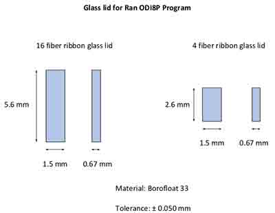
I was provided your contact information from a colleague. Does University Wafer's provide only whole wafers, or can you dice them into smaller "glass" blocks? We are presently working with several customers in the the Silicon Photonics market, and for some of our packaging assemblies we require small glass blocks. I've attached a drawing of the dimensions we are looking for, please let me know if this is something you can support.
Reference #260886 for specs and pricing.
What is an Optical Transistor?
An optical transistor is a device that uses light and electricity to switch information. The switching takes place in  a microcavity, which is a 35-nanometer-thick organic semiconducting polymer sandwiched between two highly reflective inorganic structures. The microcavity is specifically designed to favor light-matter coupling, which is the basis of this new device. Photons are strongly coupled to bound electron-hole pairs and excitons, which are short-lived quasiparticles.
This device works with photons instead of electrons, and it is capable of building an optical digital computer. Single-photon optical transistors can be used for quantum information processing, as they are capable of selectively addressing qubits. Another benefit of an optical transistor is that they are theoretically impervious to high radiation levels that can be found in outer space and on extraterrestrial planets. The same problems that plague electronic transistors also affect optical transistors.
Although an optical transistor is an analog to an electronic transistor, it does not require electrical power to operate. It uses pumped lasers to convert light into electricity. An optical transistor has a 400-480 nanometer wavelength and continuously modulates between high and low outputs, which are translated into logical 1s and 0s. It also includes a second, smaller laser beam that acts as an electronic gate, switching an incoming light from the pumped laser on or off.
Silicon Photonics Optical Transistors
Intel has demonstrated the world's first practical data connection to an electrically pumped hybrid silicon laser built into an optical transistor made of silicon photonics. The leading research group in the field of nanophotonics is working on the development of a powerful, powerful and cost-effective silicon-optical transistor (SOT). [Sources: 1, 4]
The researchers say their space - temperature-optical transistors can all do optical operations at temperatures up to 0.5 degrees Celsius. They suggest that their optical transistor would be ideal for maintaining coherence and cache in multicore CPUs. [Sources: 12, 15]
The problem is that optical transistors have a number of properties when they are connected to each other in such a way that they can process information. For example, the output of an optical transistor could drive other transistors, so that a logical signal can propagate and become known. With these means, it could be possible to create optical transistors that operate at much higher speeds than their physical counterparts. Optical manipulation of optical motors as a concept has already been experimentally demonstrated. [Sources: 0, 6, 18]
Learn more about the state of the art in the field of optical transistors in a lecture that was recently held at the OCP Future Symposium. [Sources: 5]
Electrooptical materials include lithium niobate electrooptical polymers, which have been developed considerably over the last decade and have the potential to be integrated into silicon photonics. The technology has not lost its compatibility with manufacturing and therefore lags behind the use of silicon photonics at the beginning of this article. The project, called COSMICC, aims to combine CMOS electronics and silicone photonics to develop a powerful, cost-effective and high-performance optical transistor. The areas to be investigated include the integration of photonic transistors in optical materials and the use of optical fibres. [Sources: 6, 7, 11, 13]
In the not too distant future, it will be useful to shift certain functions to computing units based on hybrid optical transistors. Large optical circuits usually consist of a phased array, but their functionality is limited. These circuits are not very complex and show the integration potential of silicon photonics. In addition to the expansion and perhaps even replacement of the semiconductor transistor on the chip with an optical equivalent for even higher computing power, the actual processing will in some cases affect silicon photonics. [Sources: 8, 11, 15]
This would be an optoelectronic integrated circuit (OEIC), which would form the basis for combining photonic functionality and electronic intelligence through seamless integration. Optical transistors connect fiber optic cables with electronics that require coupled photodetectors, LEDs and lasers. These miniaturized optical compounds will be silicon-based photonics and will have the ability to heterogeneously integrate propulsion electronics and lasers on the same substrate. Wafers for scaling - up integration of photons and electronics can prove to be an important step in the development of high-performance, cost-effective and efficient optical systems. It can be speculated that this technology could close the gap between silicon-based and silicon-optical electronics, as well as between optical and semiconductor electronics. [Sources: 2, 5, 13, 16]
It remains questionable whether optical processing can reduce the energy required to switch a single transistor, which is lower than that of an electronic transistor. To be competitive with today's electronics, optical transistors would have to perform logical operations with only a few hundred photons. This requires an integrated photonic circuit that combines various silicon photonics components and requires a large number of photodetectors, LEDs and lasers, as well as a wide range of optical components. [Sources: 2, 13, 19]
An example of heterogeneous integration would be lasers that cannot be manufactured directly from silicon, but from a combination of photodetectors, LEDs and other photonic components. [Sources: 6]
In addition, optical transistors that work with a single photon could form the basis for quantum tunnelling, which can be used to selectively address individual units of quantum information, known as qubits. There are more sophisticated applications for optical transistors, but as technology and technology improves, they may be able to build quantum tunnels in which photons do not form quantum tunnels. Similar to transitors in integrated circuits, we hope to use transits in lasers for electrooptical integrated circuits, "Feng told OpenMind. With increasing technology and improvements in technology, an optical transistor could be so much more powerful that it can make a significant contribution to the development of powerful quantum computers. [Sources: 2, 9, 17]
The purpose of optical integration is to take advantage of the cost advantage associated with using silicon as the primary material for optical transistors, and putting everything into silicon is a cost-effective solution to the problem of low-performance electronics. One of the major disadvantages of using a single photon instead of a large number of photons is that the wavelength of light is too large for electronic solutions such as transitors and modulators. Compared to electrons, only a small amount of energy is available in the photon, which can be used as a component of an optical integrated circuit. [Sources: 10, 14]
In the short term, silicon photonics chips are used in high-speed signal transmission systems that far exceed the capacities of copper cabling. Inphi is investing heavily in silicon photonics to complement the company's current portfolio of optical transistors and photonic chips and accelerate this transition. This will further drive platform innovation and new solutions in the coming years, "said the Vice-President of GF. [Sources: 3, 5, 8]
Sources:
[0]: https://www.materialstoday.com/electronic-properties/articles/s1369702114000819/
[1]: https://www.photonicsviews.com/planar-systems-for-optical-transistors/
[2]: https://en.wikipedia.org/wiki/Optical_transistor
[3]: https://www.globalfoundries.com/news-events/press-releases/silicon-photonics-marriage-optical-and-digital-gfs-rf-process
[4]: https://www.anandtech.com/show/3834/intels-silicon-photonics-50g-silicon-photonics-link
[5]: https://www.inphi.com/highly-integrated-silicon-photonics-light-engines-in-high-speed-data-transport/
[6]: https://www.optics.arizona.edu/research/faculty-specialties/photonics/glossary
[7]: http://www.gazettabyte.com/home/2015/6/2/moores-law-and-silicon-photonics.html
[8]: https://searchdatacenter.techtarget.com/feature/Understanding-silicon-photonics-technology
[10]: https://www.fibereality.com/blog/knocking-of-silicon-photonics-now-mainstream/
[11]: https://onlinelibrary.wiley.com/doi/full/10.1002/lpor.201700237
[12]: https://m-cacm.acm.org/news/238930-organic-optical-transistor-outperforms-silicon/fulltext
[13]: https://idstch.com/technology/ict/silicon-photonics-enable-large-data-centers-real-time-cloud-computing-big-data-analytics-exascale-supercomputers-cognitive-computing/
[14]: https://sciencex.com/news/2020-05-powering-bitcoin-silicon-photonics-power.html
[15]: https://arstechnica.com/science/2019/04/the-future-of-high-speed-computing-may-be-larger-cpus-with-optics/
[16]: https://www.phiconference.com/market/comparison-between-inp-and-silicon-photonics/
[17]: https://www.bbvaopenmind.com/en/technology/future/optical-computing-solving-problems-at-the-speed-of-light/
[18]: https://electrosome.com/optical-transistors-silicon/
[19]: https://medium.com/@LightOnIO/lightons-summer-series-2-optical-computing-a-new-hope-859ff43e2318


 a microcavity, which is a 35-nanometer-thick organic semiconducting polymer sandwiched between two highly reflective inorganic structures. The microcavity is specifically designed to favor light-matter coupling, which is the basis of this new device. Photons are strongly coupled to bound electron-hole pairs and excitons, which are short-lived quasiparticles.