We are a research group at Rice University (Link Research Group) and are trying to fabricate nanoparticles with a recently developed printing technique. For that, we need substrates with very low surface roughness, ideally Ra < 5 nm. We would also for both the fabrication process and subsequent imaging via SEM need the substrate to have a low electric resistivity and be somewhat conductive. We were told to look into your silicon products as a starting point, as those have worked well for the developers of the technique in the past. Would you be able to recommend and silicon substrates that would match this description? We usually work with substrates of square dimensions, but would be open to other shapes, as well. Thank you very much for your help! All the best. (261571)
What are Silicon Wafers Used For?
What are Silicon Substrates Used For?
Silicon wafers, also called silicon substrates are used for integrated circuits (IC) photovoltaic solar cells. Silicon wafers are indespensible in semiconductor and electronics fabrication. Only the highest quality silicon wafers can be used in ICs while lower quality silicon is often used for solar cells. Why? IC require highly polished silicon wafer surface. Solar cells require unpolished or as-cut silicon. Polished silicon would reflect the sun, as-cut wafers absorbe the solar rays.
The semiconductor industry generates greater $300 Billion annualy in gross sales. The majority of sales are associated with silicon. A hiccup in this industry, say if Moore's Law is finally reached then a collapse in the global economy could happen and quickly!
Below are just some of Silicon Wafer Real-World Uses
- Autos - sensors etc.
- Cameras CMOS
- Diplays
- Cell Phone Chips
- Computer Chips
Get your Si Wafer quote FAST!
What Applications Are You Using your Silicon Wafers for?
Let us know what you use your silicon wafers for and receive a 5% discount off your order.
What are Silicon Wafers Physical Properties?
See below for silicon properties.
| Density, g/cm3 | 2.329 |
|---|---|
| Melting point, °C | 1412 |
| Molecular weight | 28.09 |
| Surface tension, liquid at mp, mN/m | 736 |
| Thermal linear expansion @25°C | 2.55 x 10⁻⁶ |
| Thermal conductivity @27°C, W/(m x °C) | 159 |
| Specific heat capacity (solid), J/(kg x °C) | 712 |
| Thermal coefficient of refractive index @ 25°C | 1.50 x 10⁻⁴ |
| Modulus of rupture, MPa | 125 |
| Mohs hardness | 7 |
| Young modulus (E), Pa | 1.89 x 10¹⁰ |
| Shear modulus (G), Pa | 7.99 x 10¹⁰ |
| Poisson ratio | 0.266 |
| Solubility in water insoluble | Insoluble |
What is the Silicon Wafer Refractive Index?
Below is the refractive index of silicon wafers.
According to the formula

where e0 = 11.67 is static permittivity, refractive index of
silicon tends to 3.416, when wavelength tends to infinity
(to 1000 μm and more in our case).
Silicon Refractive Index vs Wavelength.
| μm | n | μm | n |
| 1.40 | 3.4900 | 5.83 | 3.4241 |
| 1.50 | 3.4841 | 5.92 | 3.4239 |
| 1.66 | 3.4700 | 6.00 | 3.4238 |
| 1.82 | 3.4600 | 6.50 | 3.4232 |
| 2.00 | 3.4561 | 6.92 | 3.4228 |
| 2.50 | 3.4431 | 7.00 | 3.4227 |
| 3.00 | 3.4360 | 7.14 | 3.4226 |
| 3.30 | 3.4326 | 7.30 | 3.4225 |
| 3.50 | 3.4317 | 7.50 | 3.4224 |
| 4.00 | 3.4289 | 7.72 | 3.4222 |
| 4.50 | 3.4270 | 8.00 | 3.4220 |
| 5.00 | 3.4256 | 8.16 | 3.4220 |
| 5.19 | 3.4200 | 8.50 | 3.4218 |
| 5.50 | 3.4246 | 9.00 | 3.4216 |
| 5.70 | 3.4243 | 9.09 | 3.4215 |
Silicon Wafer Electrical Properties
Below is a table shows the electrical properties of silicon.
| Intrinsic resistivity, kOhm x cm | 240 | |
|---|---|---|
| Intrinsic electron drift mobility, cm2/(V x s) | 1500 | |
| Number of intrinsic electrons, cm-3 | .22 x 1010 | |
| Ohm x cm (n-type), 1015/cm3 | 2.93 | |
| 1 Ohm x cm (p-type), 1015/cm3 | 7.33 | |
| Intrinsic hole drift mobility, cm2/(V x s) | 600 | |
| Band gap, minimum, eV | 300 K | 1.14 |
| 0 K | 1.17 | |
Silicon-Silicon Direct Bonding Using High-Temperatures
Using only high-temperature treatment, two silicon wafers can be simply bonded together. Tthe process is called silicon-silicon direct bonding. This saves on processing costs as there are no adhesives or external electric field used.
This bonding technology is called silicon-silicon direct bonding (SDB—Silicon Direct Bonding) technology.
The silicon-silicon direct bonding process is as follows:
(1) Immerse the two polished silicon wafers (either oxidized or unoxidized) in the solution containing them;
(2) Laminate the polished surfaces of two silicon wafers together at room temperature;
(3) The bonded silicon wafer is subjected to high temperature treatment for several hours in an oxygen or nitrogen environment, thus forming a good bond.
Silicon wafer bonding technology is the process of binding silicon wafers tightly by chemical and physical effects. Wafer bonding is used in MEMS processing technology and is often combined with other chemical bonding technologies such as silicon oxide bonding (SODI) and semiconductor bonding.
Common silicon wafer bonding technologies include silicon oxide bonding (SODI), semiconductor bonding and silicon nitride bonding.
Gold and silicon-utecticity bonds are often used for packaging microelectronic devices. Gold - Silicon solder is used for sintering the sintered foot, and this technology has been used for pressure transmitters since 1979.
In this process, an intermediate layer is usually placed between the two parts to glue and heat them up. The gold-silicon mixture binds to the silicon on the wafer to achieve a two-phase silicon saturation state in its two-phase system (see Figure 1). Gold - Silicon soldering is one of the most common types of wafers for sintering and sintering in the electronics industry.
Many micromachining processes are carried out at low temperatures, and this technology can be used to bond silicon to the wafer. However, gold is fixed in the centre of the silicon using recombination, which can significantly shorten the life of minority carrier silicon.
This type of silicon-silicon bond causes stress due to thermal annealing deviations, and temperature should be controlled during bonding. In general, silicon dissolves into liquid gold, but the gold does not penetrate into the silicon. Therefore, temperatures should not be high enough to dope gold onto a silicon wafer.
Finally, we added mass to the Compact, placed two silicon wafers on a heater and glowed them at a temperature of 1,000 degrees Celsius. This is because the SiO2 layer adheres better to titanium foil, which is why bonding time and temperature are crucial. Our experiments showed that the bonding surface was 90% at the annealing temperature and that the gold glowed at 100% of its potential.
Silicon Wafer Chemical Cleaning
Wafer cleaning is the removal of invisible contaminants (atoms and ions) and there are many methods, including the use of hydrogen peroxide, hydrogen sulphide and other chemical cleaning methods. The cleaning method of the hydrogen peroxide system has a good effect and is not very harmful to the environment.
It has been shown that the hydrogen peroxide system is best suited to purify silicon wafers, but the chemical reagents used can be completely volatile (H2O2, NH4OH, HCl) and the general method is to purify the silicon wafer first. If the silicon disc is cleaned with H 2SO4 (h2o2), it remains in the same condition as when used with an acid-cleaned solution from which the latter cannot be removed by a chemical cleaning method.
To clean a silicon wafer with the h2o2 system, no other reagent is required than the hydrogen peroxide (H2O2) system.
Electrostatic Bonding of Silicon Wafers Quality
(1) Thermal expansion coefficients of the two electrostatic bonding materials need to be matched, if not the substrates will be broken due to the large internal stress during the cooling process of the bonding.
(2) The anode shape affects the bonding of point contact electrodes and parallel plate electrodes. If the electrode is in point contact, there will be no pores in the bonding interface, but for the double parallel plate electrode, there will be some pores in the bonding body interface, and the bonding rate is faster than the former.
(3) The wafer surface condition affects the bonding force. The quality of the wafer bond depends on the surface of the wafers. Flatter and cleaner surfaces result in better bonding. The greater the surface fluctuation, the smaller the electrostatic attraction. The surface has the same fluctuation amplitude, and the smoother the fluctuation, the greater the electrostatic attraction.
The upper limit of the voltage during electrostatic bonding is that the glass is not broken, and the lower limit is that it can cause the elastic, plastic or viscous flow of the bonding material to deform, which is conducive to bonding. When silicon/glass bonding, the thickness of the oxide layer on silicon is generally less than 0.5mm.
Electrostatic bonding technology can also be applied to the bonding between metal and glass, FeNiCo alloy and glass, and metal and ceramic.
Bonding Wafer Chemistry & Physics
Silicon wafer bonding technology is the process of binding silicon wafers tightly by chemical and physical effects. Wafer bonding is used in MEMS processing technology and is often combined with other chemical bonding technologies such as silicon-to-silicon (S-S) bonds, but also with the use of other materials.
Common silicon wafer bonding technologies include silicon-to-silicon (S-S) and S-S bonds with other materials such as ceramics and polymers.
Gold - Silicon utecticity bonds are often used in the packaging of microelectronic devices, and this technology has been used for pressure transmitters since 1979. Gold - Silicon brazing is used for sintering the die base and for the production of silicon wafers and other electronic components.
In this process, an intermediate layer is usually placed between the two parts to glue and heat them up. Gold - Silicon soldering agent is a two-phase process with two phases, one for silicon and the other for gold. The gold-silicon mixture is bound to a silicon wafer to achieve a saturation state of silicon in a gold-silicon two-phase system (see Figure 1).
This technology allows silicon to be bonded to a wafer, and many microprocessing processes are carried out at low temperatures. Gold, however, tends to recombine in the center of silicon, which can significantly shorten the life of the minority carrier silicon.
This type of silicon-silicon bond causes stress due to thermal annealing deviations, and temperature should be controlled during bonding. There are two types of gold - doped silicon wafers, one with gold and one without gold. In general, silicon dissolves into liquid gold, but gold does not penetrate into silicon, so it is not necessary to dose gold into the silicon on the wafer.
Finally, we added mass to the Compact and placed the two silicon wafers in a heater, and the adhesive area was embedded at 90% annealing temperature. The experiment shows that bonding time and temperature are crucial, but there is a SiO2 layer that adheres better to titanium foil. At the end of the bonding process, the gold-doped silicon bond glows brightly in the heat.
Silicon Wafers Used for Substrates for Optical Filters in Transmission
Researcher:
I am looking for optical quality 4 inch Silicon wafers. Double side polished. Thickness: 1 mm. The silicon wafers will be used as substrates for optical filters in transmission. On you web-catalog I only find 0.5 mm. Would also 1 mm be available?
UniversityWafer, Inc. Supplied:
Optical quality 4 inch Silicon wafers. Double side polished. Thickness: 1 mm. Others are not as important.
Contact us for pricing.
Substrates With Low Surface Roughness
UniversityWafer, Inc. Replied:
The Si wafer surface roughness is guaranteed by repetition of the chemical-mechanical-planarization (CMP) polishing process, not by any measurement, which would be destructive. For the polished side of the wafers the normal roughness value is <0.5nm. The CofC doesn't mention any surface roughness measurements data as the roughness is guaranteed by repetition of the chemical-mechanical-planarization (CMP) polishing process.
The wafers are ready for immediate delivery.
Researcher purchased:
Silicon Wafer Item #3105
25.4mm P/Boron <100> .01-.05 ohm-cm 500um DSP Test Grade
What are Silicon Wafers Used For?
Silicon wafers are used primarily in the manufacturing of semiconductor devices, which are the fundamental building blocks of modern electronic devices. Silicon wafers are at the heart of building tiny yet powerful computer chips, harvesting solar energy, crafting minute sensors for various gadgets, illuminating our world with LEDs, and ensuring that electricity is efficiently distributed in electronic systems.
-
Silicon slices are most commonly transformed into complex microchips that serve as the brains of countless gadgets we use every day. Microchips, those tiny brains within gadgets, are nestled in numerous tools we use daily, from our computing devices and mobiles to domestic machines and the electronics that steer our vehicles. The silicon wafer acts as the substrate on which the intricate patterns of the IC are fabricated.
-
Solar Cells: Silicon wafers are also used in the production of solar cells. Solar panels harness the sun's energy using cells commonly crafted from silicon, a substance adept at transforming light into electrical power.
-
Tiny machines and various kinds of sensors, such as those that measure pressure, tilt, and spin, are typically crafted on silicon discs. Silicon-based gadgets like accelerometers and pressure sensors are tucked into cars, our pockets within phones, and even in healthcare equipment to help everything run smoothly.
-
Crafted from silicon slices, these optoelectronic tools encompass glowing diodes, light beam projectors, and photon detectors. Optoelectronic mechanisms, such as LEDs and laser diodes, serve crucial roles in the realm of digital communication, visual displays, and innovative illumination solutions.
-
Power Devices: Silicon wafers are used in the manufacturing of power semiconductor devices, which are essential for power management in various electronic devices and power systems.
Silicon's unique qualities, such as its ability to conduct electricity just right, wide availability, and cost-effectiveness make it the go-to material for crafting the heart of our electronic world. The manufacturing process involves several steps, including doping (adding impurities to change electrical properties), oxidation, photolithography, etching, and metallization, to create the desired electronic circuits and components on the wafer.
What are Some Silicon Wafer Applications?
A physicist requested help for his low frequency <5GHz research.
I have a question for you. I am looking for an easy source for high resistivity silicon wafers. When you make transmission line structures and want a good low loss silicon substrate, what is your favorite wafer? My application here is all low frequency stuff (<5GHz). It has been a long time since I have done anything with si wafers, and I’m not sure what ‘good’ is in terms of high resistivity these days. The reason I want to do this on si is that I know my laser tool can cut it well and for this particular project that is important. Anyway, I figured you would have a default, known good source and recommendation.
Prime UHR FZ silicon is very hard to get. Honestly the higher the better. I once saw 30kOhm UHR FZ intrinsic silicon.
Reference #274168 for specs and pricing.
The semiconductor industry consists of a range of different types of silicon wafers, such as semiconductors, integrated circuits, transistors and transceivers. There are several different ways to use the n-type and p-types, each with its own advantages and disadvantages. [Sources: 4, 13]
Although silicon is the most widely used material in the semiconductor industry, it is called wafer because no crystal material is specified. Although silicon has been one of the most common materials for semiconductors and transistors worldwide for many years, silicon wafers are the crystal materials that are known as n or n And p-types of silicon. While silicon is one of the most widely used materials for silicon chips, silicon wafers are a crystal material described as n-type or p-type silicon chips. [Sources: 10]
In electronics, wafers, also called slice substrates, are crystalline silicon (C Si), which is used in the manufacture of integrated circuits and solar cells. Some are used to manufacture electronic components, the rest are mainly used as mechanical support. In electronics, the wafer is used to manufacture electronic components, but in most cases it serves as a substrate for the production of semiconductors, transistors and other electronic components such as chips and chipsets. The rest, which is essentially mechanical support, forms the basis for many electronic applications. [Sources: 6, 12]
To produce world-class silicon wafers, manufacturers rely on wafer specialists such as UniversityWafer, Inc. to help test world-class waves and support the films in a fully optimized production process. Silicon wafer beds for testing devices and semiconductor capital plants also use the process of testing silicon wafers to develop and characterize semiconductors and manufacturing processes. [Sources: 1, 8]
What are Mechanical Grade Silicon Wafers?
Mechanical silicon wafers can be used for process development applications that are not sensitive to particles and surface defects. While glass wafer substrate manufacturing is most commonly used to manufacture glass wafers and silicon wafers for the MEMS and semiconductor sectors, fully customizable process designs can also handle the manufacture of wathers for applications such as high-performance electronics, advanced photonics and nanotechnology. We also offer a wide range of specialized services, including the development and production of glass and silicon substrates as well as the production of high quality silicon and glass substrate products. [Sources: 0, 8, 11]
What are Gold (Au) Coated Silicon Wafers?
For example, gold-coated silicon wafers can be used to produce composites that are manufactured with absolute precision. This means that the production of a laminated SOI wafer with a highly resistant silicon wafer, which is derived from the base of the wafer, can not only be the best, but can also enable the production of epitaxial wafers that form the high resistance of silicon wafers obtained. These excellent properties are combined with the fact that they are manufactured using the most modern inventive methods and can, for example, offer high performance in terms of high resistance to particles and surface defects, as well as high strength. Gold-coated silicon wafers can also be used to manufacture a wide range of materials such as copper, silver, copper oxide and gold, provided the composite is constructed with absolute precision. [Sources: 5, 7]
In addition, technological advances in consumer electronics will create several opportunities for silicon wafer suppliers in the near future. North America and Europe are expected to take a leading role in market share due to growing demand from established players such as Intel, Samsung Electronics and Microsoft. Qualcomm Inc's growing demand for high-performance, low-cost, high-quality silicon products in electronics and other industries in these regions will again drive growth in the global silicon wafer market over the forecast period. [Sources: 2, 13]
Where Does The Military Purchase Silicon Wafers and Other Substrates?
UniversityWafer, Inc. has been selected by some of the leading military companies for its high-performance and cost-effective silicon wafer products for the U.S. Air Force, Navy, Marine Corps and other military applications. It also works closely with the largest medical electronics manufacturers in the country, providing the highest quality and most cost-intensive effective medical and medical electronics products, and providing America's leading research and science universities with a wide range of advanced medical, medical, and biomedical applications for medical devices. [Sources: 0]Silicon wafer suppliers produce and sell bare, raw silicon wafers, and the fab and end users use them. Integrated circuits can be manufactured with a variety of different silicon types, such as copper, copper oxide or silicon on a chip. The device manufacturer simulates the performance of an integrated circuit using silicon test waves using automation and hardware. In some cases, integrated circuits are made from the same silicon as would be used in a simple silicon wafer, but they are manufactured differently from what would have been used in a flat - bottom, bare - top - bottom, single-layer - silicon circuit. [Sources: 8, 9, 12]
Micro-grinding technologies offer a wide range of applications in electronics, silicon wafer recovery, wire coating removal, capacitor cutting and more, and silicon reuse and processing. [Sources: 3]
Particle - Grade Process Test Wafers, also known as Particle Test Monitors, are silicon wafers designed for particle measurement applications. There are three additional classifications of premium wafers for specific process applications, and there are no silicon process test wafer classes on the US market. [Sources: 8]
Sources:
[0]: https://www.syagrussystems.com/industries-served
[1]: https://www.globenewswire.com/news-release/2020/08/13/2078320/0/en/Pure-Wafer-s-Announces-wafersontheweb-com-Largest-Selection-of-Prime-and-Test-Grade-Silicon-Wafers-for-Semiconductor-Fabrication.html
[2]: https://www.transparencymarketresearch.com/silicon-wafer-reclaim-market.html
[3]: https://www.airbrasive.com/reclaiming-silicon-wafers-with-the-help-of-micro-abrasive-blasting/
[4]: https://content.sciendo.com/view/journals/emj/11/2/article-p87.xml?language=en
[5]: https://patents.google.com/patent/US8252404B2/en
[6]: https://en.wikipedia.org/wiki/Wafer_(electronics)
[7]: https://www.platypustech.com/gold-coated-silicon-properties-applications
[9]: https://semiengineering.com/mixed-outlook-for-silicon-wafer-biz/
[10]: https://www.utmel.com/blog/categories/semiconductor/analysis-of-semiconductor-wafers
[13]: https://www.marketresearchfuture.com/reports/silicon-wafers-market-2052
How Silicon Wafers Are Used For Nanotechnology Research
When it comes to nanotechnology, the use of silicon wafers in research and development is essential. The  large size of silicon wafers makes it easy to perform complex experiments with them. But how is this material processed? It is made using two different methods: electron-beam lithography and thermal evaporation. The former method uses a high-pressure gas to etch patterns on the surface, while the latter uses a focused ion beam.
Silicon wafers are also useful for making nanodevices. They are shaped as a cylinder, which makes them easier to bend and form. The elliptical shape of the spheres makes them good for biosensors. The cylindrical shape of the sphere is also good for this purpose. Lastly, thin wafers can be etched to make them suitable for nanotechnology research.
Researchers may also make use of larger wafers. These can be used in nanotechnology research. The size of silicon wafers is an important consideration for this type of research. Larger diameters enable greater throughput and reduce cost. While 300 mm wafers are difficult to make, Intel is currently investigating 450 mm diameter silicon chips. These are not yet ready for commercial production, but they are essential for this type of research.
Aside from allowing nanodevices to be manufactured more efficiently, ultra-thin silicon wafers can be used in the solar energy industry. These are an important component of low-cost solar cells. The use of these wafers for nanotechnology research will open the door for even more development in the field. In addition, they can be used for a variety of purposes, including medical devices and consumer electronics.
Semiconductor wafers are typically made from crystal materials with a diamond-cube structure. In this process, crystals align according to the Miller index, determining their electrical and structural properties. During epitaxy, a single silicon wafer contains a single layer of semiconductor material. The other side of the silicon-wafer is the bonded layer. This layer is called an epiwafer.
The use of silicon-based materials is critical to nanotechnology research. It is widely used in various industries and has numerous benefits for humans. Because of its availability, silicon-based materials are the preferred material for making devices. Its use has paved the way for technological advances. In fact, this material is now being incorporated into more products and gadgets. But despite these advantages, there are some disadvantages, which make the material more valuable to nanotechnology research.
In addition to using thin silicon-based materials for nanotechnology, they are also used in electronics. They are used in various power devices and CMOS image sensors. The technology has also found uses in IT & telecom, consumer electronics, and automotive. For instance, a silicon chip can be a very powerful tool for electronic components. Its high-quality properties are also crucial in the development of a device.
The scalability of thin silicon wafers is crucial in many areas of nanotechnology research. Because it is inexpensive to produce, it can be used for high-end electronics. Moreover, it is widely used for a variety of other types of devices. But the main use for these products is in semiconductors. These devices are very common today, as they have a vast range of applications.
Silicon wafers are also used in many types of semiconductors. The most common is the degenerated silicon wafer, which has higher percentages of dopant. These are also used in MEMS processing technology. Some other types of silicon wafers include polished, epitaxial, and SOI. However, silicon is the best semiconductor. Its high mobility makes it the perfect material for semiconductors.
The surface roughness of the silicon wafers is not important. In most applications, it is the semiconductor material that is used. The surface roughness of Si is typically less than 0.5 nanometers. Therefore, it is important to check the smoothness of the silicon wafers prior to their use in a semiconductor. In the case of nanotechnology, the underlying material is not a barrier.
Silicon Wafers Used In Nanotechnology Video
Watch https://www.youtube.com/embed/N0jOpaxvLi4
Would you upgrade your current computer if it provided no increase in performance? Would companies  update server farms if yesterday's technology is just as good? Would you pay ten times the amount for a computer or mobile device with new composite chips that may replace silicon chips? Probably not. This could rapidly slow computer upgrades and replacements and could conceivabally throw the world into a recession or worse. This potential tech correction would be larger than the dot.com bust of the early 2000s.
So what uses are so important that the world cannot live without it?
For starters your phone's microchips. 
Your current vehicle's sensors.
The future Driverless vehicle sensors.
Why Use Silicon for Diffraction Gratings and Grisms?
A researcher recently procured the followng silicon ingot for micromachining silicon diffractive optics and silicon grisms for space observatories.
150mm Undoped (111) FZ >8,000 ohm-cm 300mm in length
Silicon is stable at very cold or cryogenic temperatures that is required to work in the infrared. Silicon’s high refraction index (3.4) is a great transmission in the 1.1-7 micron range is great for gratings and grisms for spectrographs that operate in the near infrared (NIR). Silicon is also ubiqutous and tooling and experience readily available.
These devices offer substantial advantages in compactness, formatting, and efficiency over other dispersive devices. For example, high-resolution spectrographs designed around immersion gratings can have volumes an order of magnitude smaller than comparable instruments built around conventional gratings. In addition, the ability to make coarse grooves using micromachining allows us to produce gratings that make it possible for the first time for infrared instruments to have continuous wavelength coverage over large bands at high resolution.
Silicon Grisms
Grisms are dispersive transmission optics that are often used in instruments that combine imaging and spectroscopy. The resolving power of devices with the same opening angle depends on the refractive index of the substrate as (n-1). Silicon grisms of a given size have resolving powers 3-4 times greater than those of grisms made from glass or other low index materials
Publications
Fabrication and test of silicon grisms for JWST-NIRCam
Silicon immersion grating spectrograph design for the NASA Infrared Telescope Facility
What Silicon Wafers Can Be Used for Scanning Electron Microscope (SEM)
Researchers have used the following substrate for their SEM experiments.
150mm N/As [100] 675um SSP 0.001-0.005 ohm-cm SEMI 1Flat (57.5mm) Thermal Oxide 0.1μm±5% thick, Empak cst
What Silicon Wafers are Used for Raman
Researchers have asked us the following: I am looking to buy Si wafers for Raman, SEM, and AFM. I was told to get some with a 300nm oxide layer, single side polished, and I want either 2- or 3-inch diameter. I am having trouble picking which ones to get, and I don't know how to tell if it has an oxide layer and how thick it is. Is this something you can help me with?
have used the following Si Wafers for Raman experiments.
76.2mm P/B (100) 380um SSP 10-20 ohm-cm SEMI Prime, 2Flats DRY Thermal Oxide (5-7)nm thick, on both sides
What Silicon Wafers are Used for Atomic Force Microscopy (AFM)
Researchers have used the following Si Wafers for Atomic Force Microscopy experiments.
50.8mm N/As (100) 380um SSP 0.001-0.005 ohm-cm SEMI Test, TTV<5μm, 1,000A oxide on both sides
Please let us know if you have any questions?
What Wafer Specs are Used to Research-Transferred Substrate Mechanical Support
Client's have used the following item for their mechanical supports.
Si Item #446
50.8mm N(100) 0-100 ohm-cm
300-350 um SSP Test Grade
What Silicon Is Used in Quantum Devices?
Silicon has proven to be a promising material for a wide range of technologies, including quantum devices. In recent years, researchers have also been investigating the possibility of using individual artificial atoms to increase the efficiency of silicon-based integrated quantum circuits (qubits). However, isolated qubit optical interfaces in silicon have proved difficult to achieve so far.
Recently, individual optically active artificial atoms were isolated in silicon for the first time. The work, published in Nature Electronics, could have important implications for future silicon-based quantum optics devices such as quantum optics and quantum computers. Dr Yuki Nakamura, one of the researchers who carried out the study, told TechXplore: 'This study was born out of our efforts to isolate materials suitable for industrial processes.
The light emitters were found in silicon, one of the most widely used materials for quantum optics and quantum computers. The individual photons emitted by the resulting device operate at telecommunications wavelengths that are much shorter than those used to study quantum systems. This latest work by Dr. Eau and his colleagues shows that it is indeed possible to isolate individual optically active artificial atoms in a silicon - similar material.
This strategy combines concepts from the field of material technology with a specific experimental setup that optimizes the detection of individual near-infrared emitters. To effectively isolate individual artificial atoms in silicon, the researchers used a combination of high-energy photon detection and low-power quantum optics.
We first generated a low concentration of fluorescent defects in the implanted carbon atoms, "says Dr. Eau. Secondly, we have built a new confocal microscopy experiment that operates at very low power and allows the detection of individual optical active spot defects that emit very weak optical signals.
Silicon insulator wafers have a number of advantages, the most notable of which is that they can be used directly to produce high-quality photonic chips. This could eventually allow the development of a wide range of new applications in the field of photonics, such as the production of ultra-cost, high-performance, energy-efficient electronics.
Dr Eau said: "We are the first to isolate a single photon beam in silicon, one of the most widely used materials in the world for photonics. In the future, isolating individual artificial silicon atoms and introducing them to colleagues could help develop a wide range of new technologies. This could facilitate the use of integrated quantum photonic tools, for example, in which optically active defects embedded directly in a silicon quantum chip can generate photonic quantum "bits." In addition, the study could be an important step towards creating additional quantum freedoms associated with electron spin in embedded defects.
He said: "We now plan to integrate and control individual fluorescence defects isolated in silicon - based nanostructures such as waveguides - to enable the implementation of quantum photonic algorithms. In the future, coupling the emission of individual telecommunication potentials with spin control could enable a wide range of new applications in quantum computing and quantum information processing.
We also want to tackle the problem of connecting the electron spins of artificial atoms in order to implement quantum memory. In the long term, our goal is to develop a Si-based quantum spin photon interface that can be used in a variety of applications such as quantum computers and quantum information processing.
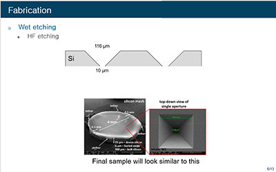
What Wafer Should I Use to Make a Silicon Mesh
A scientist requested the following:
We are looking for a 75 micrometer thick <100> undoped Si wafer (4 inch). Is it possible to purchase 75 micrometer thick wafers? I hope it is not too hard to handle because it's too thin.
Our research group is working with Si wafers for the first time, so we are not really familiar with them.
We need both sides to be really flat, so I'm guessing double side polished? We are looking to purchase 10 of them.
We need to do PECVD and KOH etching to create holes and make a silicon mesh.
The purpose of the oxide layer was just to create a mask that resists KOH. Is there also a photoresist that resists KOH?
We were planning to use KOH etching to create a square conical hole like a pyramid.
Also, can p-type wafers also create slopes of 54.7 degrees while they are etched in KOH?
If there's a photoresist that resists KOH, then I think the procedure would be:
1. Apply photoresist and create a pattern through photolithography
2. Dip it in KOH to create holes in the Si wafer
UniversityWafer, Inc. Quoted the following. Please contact us for pricing.
Item Qty. Description
GX64. 10/25 Silicon wafers, per SEMI Prime, P/P 2"Ø×75±10µm,
p-type Si:B[100]±0.5°, Ro=(1-20)Ohmcm,
Both-sides-polished, SEMI Flat (one),
Individually packed.
Step 1. Silicon Mesh Fabrication

2. Silicon Wafer Mesh Hard Mask Deposition

3. Silicon Wafer Mesh Photolithography

4. Silicon Wafer Mesh Wet-Etching

5. Silicon Wafer Mesh KOH Etching

6. Silicon Wafer Mesh HF Etching