Gallium Nitride on Silicon Bonding
A postdoc requested a quote for the following research:
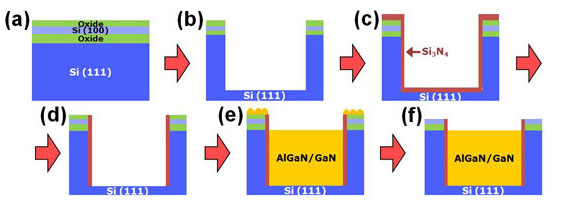
For background, our aim is to produce a GaN-on-diamond technology platform, which we will achieve through bonding of GaN-on-Si wafers to Si carriers, removal of the original substrate and then diamond growth on the exposed III-N surface. We have access to a bonding tool (and associated expertise) which can take 4” wafers only, hence the specific request.
- 2DEG properties, i.e. carrier density/mobility/sheet resistance
- Surface roughness
- Total epistructure thickness (including nucleation and strain relief layers)
As you have to removal of the original substrate and GaN layer,what's about 4'' GaN-on-Sapphire,is this applicable? this will be fast delivery from our regular production.
I hope this is somewhat useful. Please let me know if I can provide any more information, and any updates you can provide on the status of the 4” GaN-on-Si growth would be greatly appreciated.
Rreference # 245857 for specs and pricing.
Get Your GaN-on-Si Quote FAST!
Standard GaN-on-Si Standard Epi-Wafer Characteristics
GaN-on-Si FEATURES
- High uniformity
- Low leakage current
- Higher operating temperatures
- Excellent 2DEG characteristic
- High breakdown voltage (600V-1200V)*
- Lower ON-resistance*
- Higher switching frequencies*
- Higher operating frequencies (upto 18GHz)**
Typical Application
- *Power HEMT
- *RF HEMT
- *GaN Diode
| GaN Materials Specs |
Dia 150mm |
| Wafer Warp (um) |
<50 |
| AFM RM (nm) |
<0.5 |
| (002) FWHM (arcsec) |
<600 |
| (102) FWHM (arcsec) |
<1200 |
| Hall Sheet Resistiance (w-2) |
<500 |
| Hall Sheet Carrier Density, N8 (Cm2) |
>1E+13 |
| Hall Mobility, u (cm2/V-s) |
>1500 |
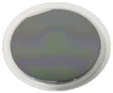
Typical GaN-on-Si Wafer

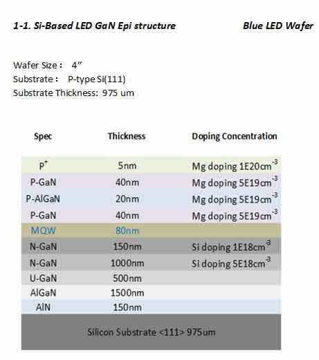
Could you give me more information on Blue/Green LED on Si?
Blue LED on Silicon wafer epi structure, Green LED epi structure are similar as it.
The surface morphology or layer quality are epitaxial growth finished for process LED chip as industrial standard.

GaN on SIlicon for HEMT
Researcher:
I'm looking for a GaN-Si Epiwafer for 650V Power HEMTs. Happy to take coupons, or 4"/ 6" wafer for now. Therefore appreciate if you can let me know price for 10 coupons, 4" and 6" wafer.
UniversityWafer, Quoted:
1. 4'' GaN-Si Epi wafer for 650V Power HEMTs,qty. 10 pcs $/ea
2. 6'' GaN-Si Epi wafer for 650V Power HEMTs,qty. 10 pcs $ $/ea
Please contact us for pricing.
Researcher:
These epi wafers are E-Mode : Enhanced Mode
D-Mode : Depleted Mode ?
E-Mode has better performance than D-Mode.
Both modes are availble.
We also have:
GaN on Sapphire
GaN on Silicon Carbide
Bulk GaN
What GaN on Si Spec is Used 650V to Fabricate Power HEMT?
E-Mode usually has better performance than D-Mode. Scientists have used the following:
Pls see below for 4'' and 6'' 650V Power HEMT GaN epi wafer
1. 4'' GaN-Si Epi wafer for 650V Power HEMTs
2. 6'' GaN-Si Epi wafer for 650V Power HEMTs
Contact us for pricing.
Will Gallium Nitride Replace Silicon Wafers?
GaN-on-Si wafers have grown in popularity in the production of High Electron Mobility Transistors (HEMT). It and related binaries InN and AlN, as well as ternary compounds. Applications include:
- light emitters of UV through green wavelengths
- optical detectors
- microwave communication
- high power applications.
Scientists have used our wafers for their GaN Nanostructures on Silicon Research.
What Are Gallium Nitride on Silicon Applications?
The bandgap of gallium nitride on silicon semiconductors is three times larger than that of silicon. This wide bandgap allows for a much wider range of voltage and temperature applications. A new bonding technique developed by researchers at the Georgia Institute of Technology makes it possible to attach wide-band gap materials to thermal conductors. The result is a higher switching rate and faster switching than silicon.
Because of its wide bandgap, the materials are useful for power-related electronic circuits, such as transistors, diodes, and integrated circuits. Silicon, which is the most common of semiconductor materials, is quickly running out of room in technology. Luckily, there are other materials available to fill this void. A recent breakthrough in silicon manufacturing has allowed gallium nitride to fill the void.
Gallium nitride on silicon (GaN) is a semiconductor with a broad bandgap. This means that the material has a wide bandgap compared to silicon. This allows it to sustain a higher temperature than silicon MOSFETs. This makes it ideal for high-frequency and high-power devices. Further, the material is more durable and able to handle a wider range of temperatures.
The popularity of gallium nitride on silicon is growing rapidly. It is 200 degrees warmer than silicon, making it more suitable for high-frequency applications. The technology behind galium nitride is more advanced and future-proof. For this reason, more semiconductor manufacturers are turning to the material as it is a much better choice than its predecessor. However, many of these products will still be made of silicone.
Another advantage of gallium nitride on silicon is its wide bandgap. This means that it has a large bandgap compared to silicon, making it perfect for high-frequency applications. Besides being widely compatible with silicon, gallium nitride on silicone is also capable of withstanding high temperatures compared to its counterpart. Despite its disadvantages, it is still an excellent choice for power conversion schemes.
In semiconductor devices, gallium nitride on silicon is one of the best choices. This material is more stable at higher temperatures than silicon, and can withstand much more energy than silicon. This property makes it a more viable candidate for high-frequency semiconductor applications. This makes it a more cost-effective option for semiconductors in power-efficient systems. If you're looking for a high-frequency device, gallium nitride on a silicon substrate might be the best choice.
Because it's a high-bandgap material, gallium nitride on silicon is a great option for high-speed data transfer and power-conversion. Its narrow bandgap also makes it more efficient than silicon, allowing it to be used in a wide range of electrical and mechanical applications. It is a great material for these applications.
Although silicon has been the standard for most tech applications, gallium nitride on silicon is rapidly making a name for itself as a viable substitute. This high-frequency semiconductor has a wider bandgap than silicon and is therefore a better choice for high-frequency products. This makes it more efficient and future-proof, as it's not only safer, but also more efficient.
Because of its unique properties, gallium nitride is an excellent semiconductor material. It has a low electrical resistance and is ideal for RF and high-frequency components. Its low cost makes it an attractive option for a wide range of electronic applications, and it is much cheaper than silicon. Its low price also makes it an attractive option for a wide variety of other devices.
Because of its low voltage, gallium nitride is the ideal semiconductor for automotive applications. Its low-voltage characteristic makes it an excellent candidate for high-power transistors. The same characteristics make it ideal for use in power converters. The latter, however, are less prone to heat and are more flexible than silicon. Its superior performance is a key factor in this technology's emergence.
Video: Applications of Gallium Nitride (GaN)
150mm DesiGaN Power/RF HEMT Series
We have a large selection Gallium Nitride on Silicon wafers available diameters 100mm-200mm. Small quantities acccepted.
IGSS GaN 150mm DesiGaN Power/RF HEMT Series of Gallium Nitride on Silicon (GaN-on-Si) is an
AlGaN/GaN hetero-epitaxial layer structure grown on a Silicon(111) substrate targeting high voltage Power & RF applications.
See below for Inventory.
Standard GaN-on-Si Standard Epi-Wafer Characteristics
GaN-on-Si FEATURES
- High uniformity
- Low leakage current
- Higher operating temperatures
- Excellent 2DEG characteristic
- High breakdown voltage (600V-1200V)*
- Lower ON-resistance*
- Higher switching frequencies*
- Higher operating frequencies (upto 18GHz)**
Typical Application
- *Power HEMT
- *RF HEMT
- *GaN Diode
AlGaN (24-28% Al / typ. 10-20nm)
GaN Channel (Typical 100-200nm)
Gallium Nitride on Silicon Inventory
We carry the following in stock. Please send us the specs and quantity you would like su to quote.
GaN-on-Silicon Wafer Series Prime grade |
Diameter |
Orient. |
Substrate Thickness |
Surface Finish |
GaN Template Thickness |
Conduction Type |
Dopant |
| 2 |
<111> |
1000+/-25um |
SSP |
100~5000nm |
N-type |
Un-doped |
| 4 |
<111> |
525~1000+/-25um |
SSP |
100~5000nm |
N-type |
Un-doped |
| 6 |
<111> |
675~1000+/-25um |
SSP |
100~5000nm |
N-type |
Un-doped |
| 8 |
<111> |
725~1000+/-25um |
SSP |
100~5000nm |
N-type |
Un-doped |
| 2~8 |
<111> |
500~1000+/-25um |
SSP |
HEMT Structure GaN |
N/S.I-type |
S.I-doped |
| 4~6 |
<111> |
500~1000+/-25um |
SSP |
Blue/Green LED GaN on Si |
N/P-type |
N/P-doped |
| 2~8 |
<111> |
500~1000+/-25um |
SSP |
100~500nm AlN |
S.I-type |
Un-doped |
Wide Bandgap Advantages of Gallium Nitride on Silicon
In this study, Gallium nitride on silicon (GaN-on-Si) is used as an electrical insulator in a power IC chip. Its 'green' features include an ultra-low carbon footprint due to its aluminum source. The use of GaN in this power IC chip saves up to 80% in manufacturing and packaging processes, and it also offers significant system-level efficiency improvements.

One of the main advantages of gallium nitride is its wide bandgap, which is related to the amount of energy required to free an electron from its orbit around the nucleus. It is also more stable at higher temperatures than silicon, which makes it ideal for high-frequency applications. In addition, it is capable of withstanding much higher temperatures than silicon. As a result, it could be used in high-power and optoelectronic devices.
The disadvantages of gallium nitride on silicon are primarily cost and size. GaN on silicon has a much lower cost of production and can be manufactured in silicon factories. The other major benefit is that GaN on silicon has a much smaller footprint and higher power density than silicon. The downside is that the cost of production for GaN is also significantly lower than for silicon. Nevertheless, it's worth the investment.
The biggest benefit of GaN on Si is its large bandgap and low cost. It can be processed with very low temperatures and allows for high-performance CMOS devices. In addition, it allows for larger diameter fabs, which can support a wider range of applications. Currently, vendors can produce about 5,000 8-inch wafers per week. The biggest challenge for the GaN on Si process is scaling the supply chain to reach the mass commercial markets.
In addition to reducing switching losses, GaN ICs also have low cost. The reduced cost is due to the lower switching frequency and lower switching resistance. In contrast, GaN ICs reduce the size of bulk capacitors and main transformers. They also help increase the switching frequency and power density. Finally, the material is a good material for LED lighting. Its high temperature is resistant to shock and is not flammable.
GaN on silicon is a type of semiconductor. It has a wide bandgap, which means that it can withstand higher frequencies and voltages. In other words, GaN on SiC is a high-tech material with a high energy-density. It is a popular semiconductor in many types of electronics, including smartphones, but also in other fields. This makes it a versatile material for a variety of applications.
Gallium nitride is a unique semiconductor material that has several advantages. For example, it can handle high power levels, and has low electrical resistance. Moreover, its cost is significantly lower than that of silicon, which makes it an ideal material for RF components. This allows for lower-power and high-speed photonics. The materials are also cheaper than silicon, which makes them attractive for a wide variety of electronic applications.
The application of gallium nitride is increasing dramatically. Compared to silicon, it is 200 degrees Celsius warmer than silicon and is better suited for high-frequency applications. In the future, high-frequency products using galium nitride will be widely available. These new semiconductors are more efficient and can handle higher loads. With these qualities, gallium nitride is a future-proof material.
Besides LED production, it is also being increasingly used in RF components and power switching. Despite its new name, it has remained a niche market in the semiconductor industry for decades. Its unique properties are what set it apart. Aside from being a very hard material, it's also highly resistant to radiation, which makes it ideal for a wide variety of applications. Its advantages make it a viable choice for power electronics.
Gallium nitride on silicon is one of the most popular semiconductor materials. It has the highest bandgap of all semiconductors. It is also used in power conversion schemes. Its high bandgap is one of the main advantages of this material over silicon. A wide bandgap is essential for a semiconductor to work effectively. The wider the bandgap, the greater the efficiency.
